Reverse Engineering of Printed Circuit Boards
Reverse engineering depicts the sequence of operation of reconstructing a complete project database. For successful reconstruction all parts used in the imported board should be defined in EDWinXP part library. From BOM that contains list of all used parts, we can find whether needed parts are already defined and what missing parts have to be added
- Sample Project details
- Reconstruction steps
- Import of ODB++ database
- Netlist Export
- Reconstruction of Library Elements
- Updation of BOM parts
- Import of ODB++ with the script
- Reconstruction of schematics
- Recreate via holes and traces from Gerber import
Sample Project details
Let us reconstruct a project with the following source files:
- Board1-odb++.zip - compressed board database in ODB++ format
- Board1.X01 - Top artwork (Gerber format RS-274-X)
- Board1.X10 - Drill (Gerber format RS-274-X)
- Board1.X11 - Contour (Gerber format RS-274-X)
- Board1.X21 - Bottom artwork (Gerber format RS-274-X)
- Board1-picture.jpg = image of the board (unpopulated)
Reconstruction steps
- Import of ODB++ database
- Reconstruction of Library elements
- Import of ODB++ with the script
- Reconstruction of schematics
- Recreate via holes and traces from Gerber import
Import of ODB++ database
- Import of ODB++ database
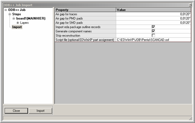
Import of each ODB++ job steps consists of three automatically following phases. Three phases are as follows.
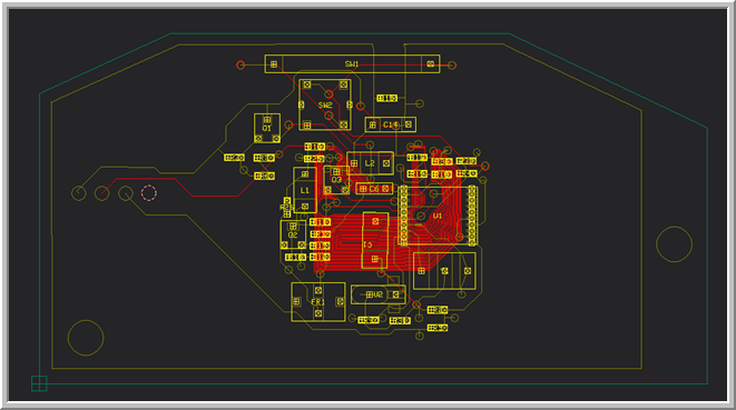
The program finds out the components used on the board and footprints and silkscreen of the required (traces and via holes)
packages during PCB layout import. The result is as follows:
Netlist Export
Exports the net list from the project in order to obtain a template for BOM. During ODB++ import, EDWinXP creates dummy parts that are named as packages. For full part description we need schematic symbol of part (for schematic view) and the package (PCB layout view).The Net list obtained is as follows:
(PATH,Board1 - ODB++ Import(MAINHIER)
(COMPONENTS
C1,1_SMD2_2
C6,1_SMD2_6
C10,1_SMD2_7
C11,1_SMD2_7
C12,1_SMD2_7
C13,1_SMD2_7
C14,1_SMD2_5
C15,1_SMD2_7
C16,1_SMD2_7
R1,1_SMD2_7
R2,1_SMD2_7
R3,1_SMD2_7
R4,1_SMD2_7
R5,1_SMD2_7
R6,1_SMD2_7
R7,1_SMD2_7
R9,1_SMD2_7
R17,1_SMD2_7
R18,1_SMD2_7
R19,1_SMD2_7
R25,1_SMD2_7
R26,1_SMD2_7
R31,1_SMD2_7
R33,1_SMD2_7
R34,1_SMD2_7
Q1,1_SMD3_2
Q2,1_SMD3_3
Q3,1_SMD3_3
L1,1_SMD2_4
L2,1_SMD2_4
U1,1_SMD20_1
U2,1_SMD2_3
FR1,1_SMD4_1
Y1,1_SMD3_1
SW1,1_SMD2_1
SW2,1_SMD6_1
)
(VALUES
C15,NONE
R2,NONE
Q2,NONE
Q3,NONE
Q1,NONE
C6,NONE
C14,NONE
L1,NONE
L2,NONE
U1,NONE
U2,NONE
FR1,NONE
C1,NONE
Y1,NONE
SW1,NONE
C13,NONE
R33,NONE
R34,NONE
R18,NONE
R4,NONE
R1,NONE
C10,NONE
R9,NONE
R5,NONE
R31,NONE
R17,NONE
C11,NONE
R6,NONE
C16,NONE
C12,NONE
R25,NONE
SW2,NONE
R26,NONE
R7,NONE
R3,NONE
R19,NONE
)
(NODES
(9
Y1,3
U1,4
)
(23
R33,2
)
(22
U1,7
R33,1
R34,2
)
(5
U1,1
R9,2
)
(4
U1,20
R2,2
R5,2
)
(21
U1,9
R18,2
)
(3
FR1,4
Q2,2
R26,1
)
(2
U1,2
U2,2
U2,1
R9,1
R31,1
)
(20
L1,2
C11,1
Q2,1
C10,1
)
(19
C6,1
R1,2
)
(15
Q3,2
R18,1
C11,2
R19,2
)
(18
SW1,2
U1,17
R4,2
SW2,3
)
(13
FR1,2
C1,1
Y1,2
U1,18
U1,16
U1,15
U1,14
U1,13
U1,12
U1,11
U1,10
Q3,3
C6,2
U1,19
C16,2
C12,2
R2,1
R1,1
R31,2
R17,2
R7,2
R19,1
C13,2
R34,1
)
(17
C1,2
U1,6
U1,5
Q1,3
R4,1
)
(12
Q3,1
Q1,1
C14,2
C14,1
L2,2
L2,1
C15,2
C15,1
R3,1
C13,1
)
($NONE$
)
(27
U1,8
)
(11
FR1,3
)
(10
FR1,1
)
(32
SW2,2
)
(31
SW2,5
)
(30
SW2,1
)
(29
SW2,4
)
(7
C12,1
Q2,3
C10,2
R17,1
)
(16
R25,2
)
(26
L1,1
C16,1
R25,1
R26,2
)
(25
R6,2
R7,1
)
(24
Q1,2
R6,1
R3,2
)
(6
R5,1
)
(28
SW1,1
SW2,6
)
(8
Y1,1
U1,3
)
(1
)
(33
)
)
(BOARDDATUM,I
0,1376,0,2022
(BOARDVERTEX X,Y,ID
0,0000,0,0000,1
0,0000,1,2400,1
0,5600,1,4950,1
2,0000,1,4950,1
2,8450,1,0950,1
2,8450,0,0000,1
0,0000,0,0000,0
)
)
(COMPPOSITIONS,I
C15,T,1,1.4518,1.2201,2,1.5090,1.2194
R2,T,1,1.6678,0.3153,2,1.7250,0.3146
Q2,T,1,1.0802,0.6723,3,1.1176,0.5926
Q3,T,1,1.2654,0.9069,3,1.3028,0.8272
Q1,T,1,0.9702,1.1278,3,1.0084,1.0469
C6,T,1,1.3801,0.8329,2,1.4729,0.8336
C14,T,1,1.4193,1.1059,2,1.5719,1.1097
L1,T,1,1.1320,0.8952,2,1.1318,0.7578
L2,T,1,1.3398,0.9426,2,1.4772,0.9424
U1,T,1,1.5529,0.6014,20,1.8418,0.6014
U2,T,1,1.4067,0.3815,2,1.5181,0.3815
FR1,T,1,1.0940,0.3503,4,1.1884,0.3014
C1,T,1,1.4284,0.5325,2,1.4310,0.6931
Y1,T,1,1.6269,0.4824,3,1.8243,0.4824
SW1,T,1,0.9986,1.3659,2,1.6661,1.3671
C13,T,1,1.5796,0.9673,2,1.6368,0.9666
R33,T,1,1.7896,0.9519,2,1.8468,0.9512
R34,T,1,1.6858,0.9499,2,1.7430,0.9492
R18,T,1,1.6844,0.8942,2,1.7416,0.8935
R4,T,1,1.7906,0.8994,2,1.8478,0.8987
R1,T,1,1.1690,0.6398,2,1.2262,0.6391
C10,T,1,1.0627,0.5409,2,1.1199,0.5402
R9,T,1,1.3731,0.2723,2,1.4303,0.2716
R5,T,1,1.6678,0.2394,2,1.7250,0.2387
R31,T,1,1.5069,0.2703,2,1.5641,0.2696
R17,T,1,1.1659,0.5903,2,1.2231,0.5896
C11,T,1,1.1669,0.6912,2,1.2241,0.6905
R6,T,1,0.9306,0.8879,2,0.9878,0.8872
C16,T,1,1.1438,1.0136,2,1.2010,1.0129
C12,T,1,1.1664,0.5419,2,1.2236,0.5412
R25,T,1,1.1419,0.9609,2,1.1991,0.9602
SW2,T,1,1.1398,1.1031,6,1.2950,1.1050
R26,T,1,1.0544,0.7248,2,1.0551,0.7820
R7,T,1,0.9283,0.9662,2,0.9855,0.9655
R3,T,1,0.8026,0.9668,2,0.8598,0.9661
R19,T,1,1.5809,0.8974,2,1.6381,0.8967
)
),Board1 -ODB++ Import
Reconstruction of Library Elements
- Import packages in recreated parts and add existing schematic symbols from EDWinXP libraries to part descriptions.
- Reconstruct parts for components on the board using Library Explorer and Library Editor.
- Extract all packages from the project library and store them in a newly created private library SCANCAD.PACKAGE.
Invoking Library Explorer:
From EDWinXP Main: System -> Library -> Explorer
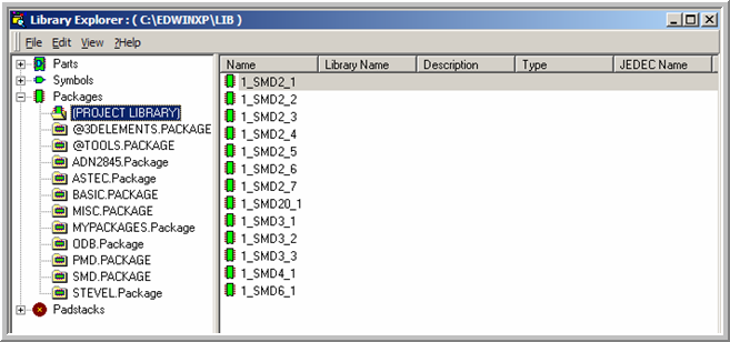
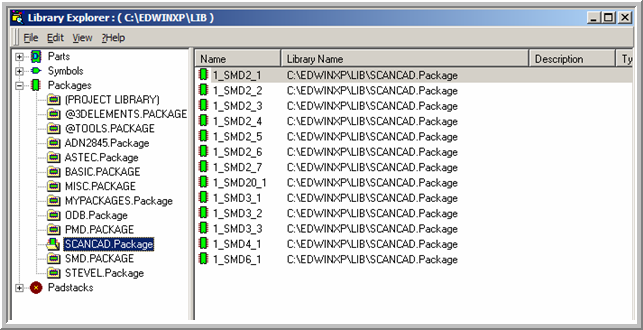
From Library Explorer: File -> New -> Package Library And using Copy and Paste copy all
imported packages to the newly created private package library SCANCAD.package.
Create empty private libraries for part descriptions – SCANCAD.Part and schematic symbols – SCANCAD.Symbol.
Assume components with C and R name prefixes respectively capacitors and resistors
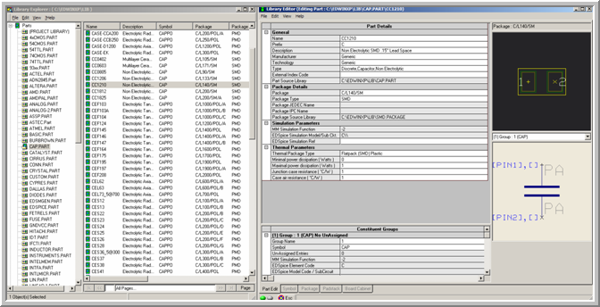
Use existing part as template and just replace referenced package:
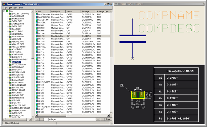
For example –select part CC1210 as template and open Library Editor
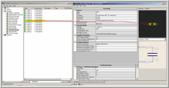
Replace current package with suitable package from SCANCAD.Package library:
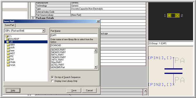
And save the updated part description in SCANCAD.PART library
Create remaining parts for the project.
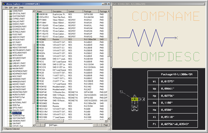
Change pin assignments for transistors because pin numbers used in EDWinXP differs from those in imported packages:
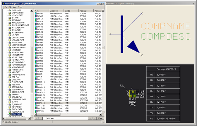
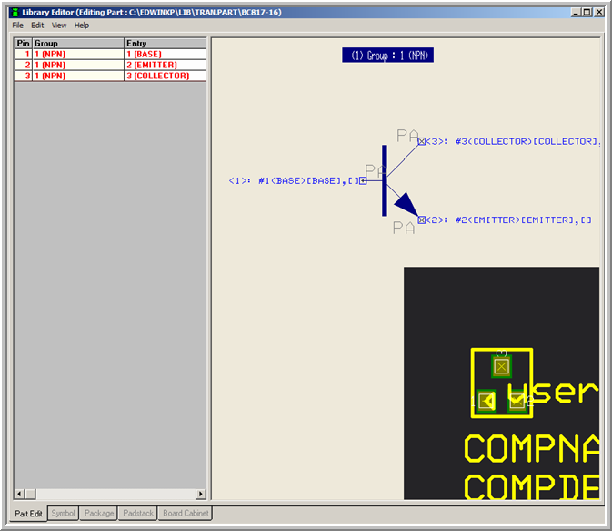
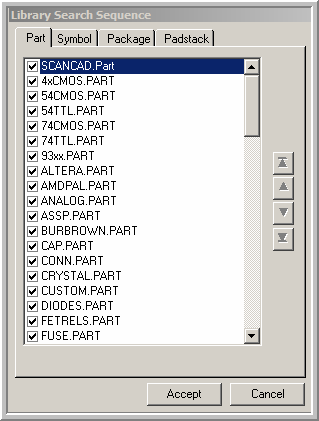
To use private libraries for this project put on top of the search sequence to ensure that when library
elements will be searched for, they will be found first in those libraries and not in system libraries.
(Use dialog invoked from Library Explorer by: View -- >Search Sequence):
Updation of BOM parts
PATH,Board1 - ODB++(MAINHIER)
(COMPONENTS
C1,CAP2
C6,CAP3
C10,CAP1
C11,CAP1
C12,CAP1
C13,CAP1
C14,CAP4
C15,CAP1
C16,CAP1
R1,RESISTOR
R2,RESISTOR
R3,RESISTOR
R4,RESISTOR
R5,RESISTOR
R6,RESISTOR
R7,RESISTOR
R9,RESISTOR
R17,RESISTOR
R18,RESISTOR
R19,RESISTOR
R25,RESISTOR
R26,RESISTOR
R31,RESISTOR
R33,RESISTOR
R34,RESISTOR
Q1,TRANSISTOR1
Q2,TRANSISTOR2
Q3,TRANSISTOR2
L1,INDUCTOR
L2,INDUCTOR
U1,CODEC
U2,SWITCH
FR1,RECTIFIER
Y1,TRIAC
SW1,POT
SW2,VOLREG
)
Import of ODB++ with the script
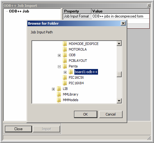
Import ODB++ with a script assigning library parts to the imported components. Since all recreated parts have references both to PCB packages and corresponding schematic symbols, this import produces complete,editable EDWinXP project. Using script is optional.
(
CAP1(C10,C11,C12,C13,C15,C16)
CAP2(C1)
CAP3(C6)
CAP4(C14)
RESISTOR,(R1,R2,R3,R4,R5,R6,R7,R9,R17,R18,R19,R25,R26,R31,R33,R34)
TRANSISTOR1(Q1)
TRANSISTOR2(Q2,Q3)
INDUCTOR(L1, L2)
CODEC(U1)
SWITCH(U2)
RECTIFIER(FR1)
TRIAC(Y1)
POT(SW1)
VOLREG(SW2)
)
Reconstruction of schematics
After import, reconstructed schematic components are placed on top of each other at the center of main page. To make a readable
schematic use auto-placer and auto-router from Schematics Editor. These routines have many features which enable fine tuning of results.
Before components are placed they have to be removed from the page to locations outside that we call BINS.
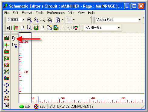
This function produces following results
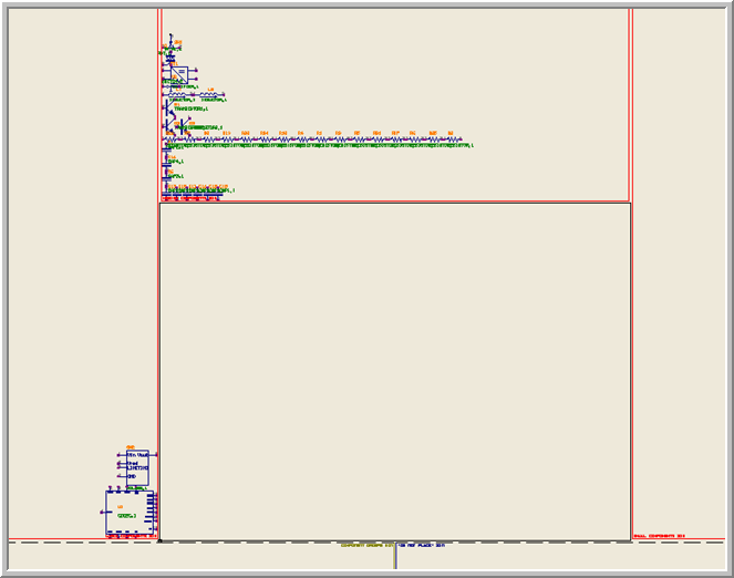
Now set up placement rules
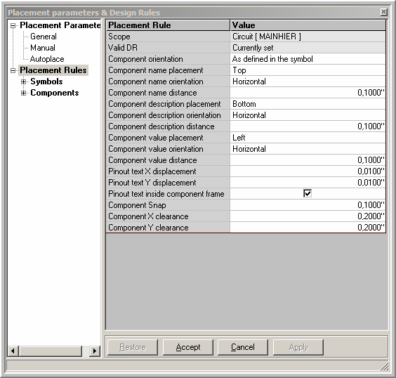
And subsequently set up placement parameters:
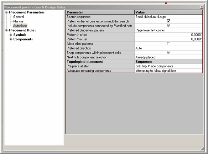
Before placement can start, at least one “strategic” component has to be placed manually on the page at desired position.
We call such component as “hub” component because remaining components will be moved from bins and placed in relation to the hub:
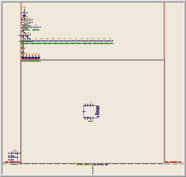
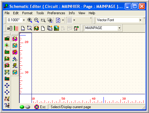
Placement is invoked by selecting tool Autoplace all components with option Autoplace starting from selected hub component and
by clicking on component at the center of the board.
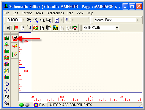
Next step after placement would be routing of wires. In the same menu, select function
Reroute connections and click option Autoconnect wires.
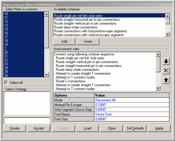
This shows the result of auto-placement and auto-routing:
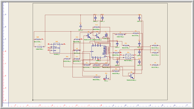
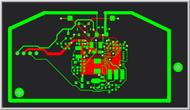
Recreate via holes and traces from Gerber import
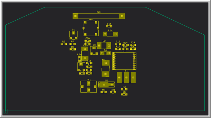
Remove all traces and other copper imported from ODB++ leaving only components:
Using Gerber Viewer import artworks for top and bottom layers:
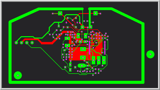
From drill file import holes – though some are missing – probably because on the picture they are filled with solder:
Gerber Viewer allows passing imported graphics to EDWinXP. Fabrication Manager
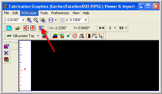
In this module we have a suite of tools for editing imported graphics and preparing them for PCB reconstruction. Imported graphics are
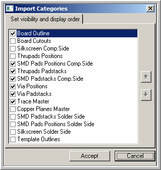
categorized. This is necessary since Gerber data are ambiguous. For example a line may be a trace segment but may also be a SMD pad.
Import process tries to categorize data as much as it can. For example graphics created with flashed apertures (D03*) are assumed to be pads.
Nevertheless some editing and manual categorization of data is in most cases necessary:
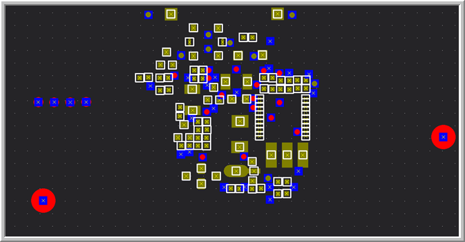
For reconstruction of vias use category Via positions as a template. Since drill file was incomplete (missing holes)
some of via pad positions were categorized as SMD pad positions. Using category to category transfer functions of Graphics
Import Editor in Fabrication Manager create a template for all vias in Via Positions category.
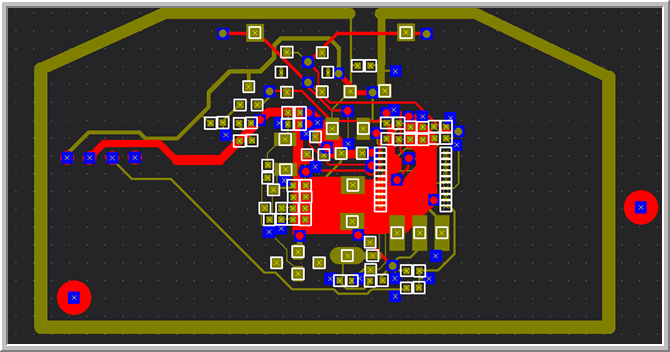
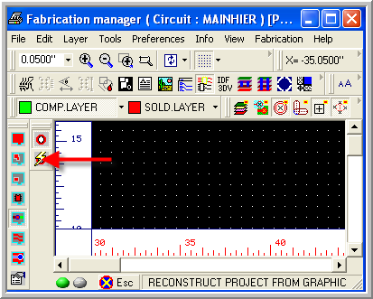
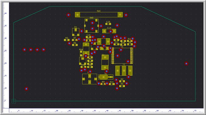
Next Reconstruct from Graphics in Fabrication Manager and reconstruct vias using automatic function.
Vias have to be reconstructed before traces.
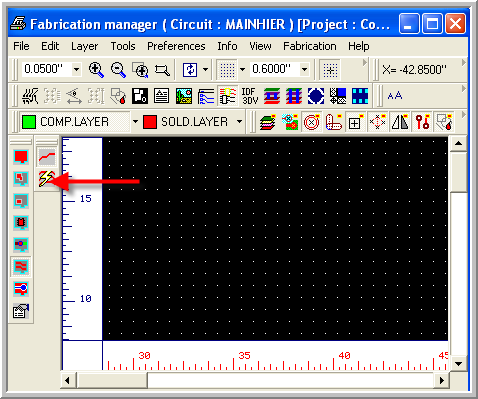
Next reconstruct traces. This is also an automatic function in Reconstruct from graphics toolbar.
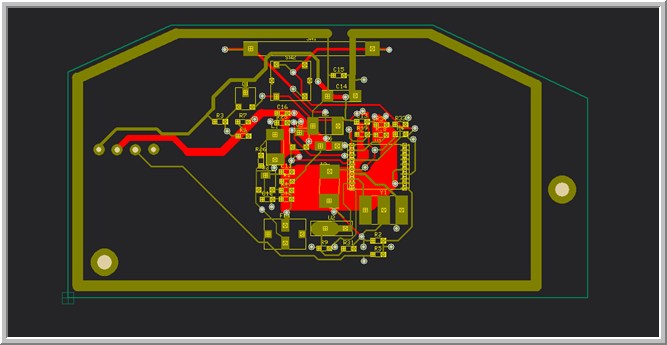
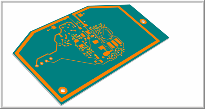
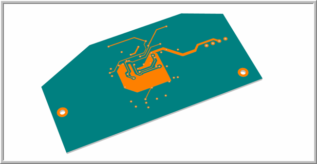
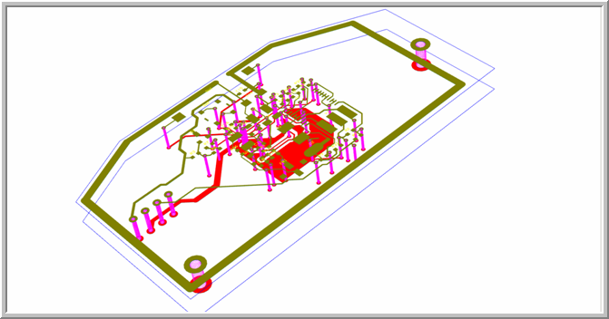
Adjust pad sizes and hole diameters for 3 different via pad stacks (in Layout Editor)to get a reconstructed = reverse engineered board:
Read More:
Introduction to Reverse Engineering
Reverse Engineering