Project Reconstruction from Netlist/Wirelist
EDWinXP PCB Wirelist (.wrl)
PCB wirelist is the layout information of a board in netlist format. This option is used to import the wirelist files (*.wrl) and can be used to construct the project database. The dictionary file and the location where the import file resides are browsed using the ellipsis. To import the contents, click the import button. This action clears the current loaded database. The report file is displayed in an ASCII viewer. We have included few new features in the PCB Wirelist Export/ Import option. It is now able to export board datum location, board details and position of each component. The board details include the XY coordinates of each vertex of the board. The component position includes the name of component, placement side on the board (top or bottom) for each PCB component and X, Y coordinates of pin #1 and pin #n. While importing the wrl file for reconstructing the project database, the board datum location is used to load the position of board. Each PCB components are placed according to the data retrieved from the PCB wire list file: position, placement layers and orientation. Board with poly shape can now be exported and imported.
How to add comments?
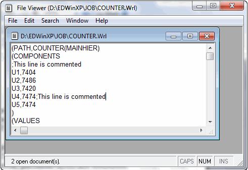
Open the PCB wire list file in notepad or in file viewer and write the comments starting with a semicolon (;).
EDWinXP Integrated Library Structure depicted in below figure.
The net/ pin connection in the layout can be automatically mapped to the schematic in EDWinXP. If you provide the schematic wirelist (.wrl file format), we can recreate the schematic from this wrl file, since EDWinXP automatically detects the corresponding schematic pins/ connections from the layout information. So generating the wrl file will be the best idea to recreate the schematic. You want to have the wrl file format compatible to EDWinXP. And the board information is to be exported to the wrl file format so that it can be reverted in EDWinXP. In EDWinXP, the Netlist/ Wirelist Export/ Import can be performed by the following formats.
- Layout wirelist which imports the layout information COUNTER(PCB layout format). Wrl – This contains the Layout information of the board, and this file is necessary for the import of layout information and hence the schematic components.
Import of PCB layout wirelist (COUNTER(PCB layout format).wrl).- Our project database is integrated, meaning that once component is added
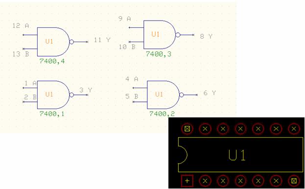
to the PCB layout, its schematic equivalent is automatically created. It applies to netlist too. The netlist is common for PCB and schematic view. This feature allows reconstructing schematics from PCB layout wirelist (and list of components there). For example – if in PCB wirelist we find 7400 component named IC1, we know that we have to add four NAND gates symbols to the schematics, packaged as IC1/1, IC1/2, IC1/3, IC1/4. Numbers after “/” denote gate numbers in the package. Pin-out information specified in 7400 part description stored in our library allows for translating package pin numbers to pin numbers in gate symbols on the schematics. Reconstruction of schematics from PCB layout wirelist involves also three steps - import, auto-placement of components and auto-routing of connections.
PCB Wirelist Import Procedure
The procedure to import a PCB Layout Wirelist file can be carried out as below
- Select Project -> Netlist/ Wirelist Export & Import from the EDWinXP Project Explorer
- Choose File -> Import Project
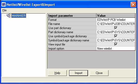
- Select Format -> EDWinXP PCB Wirelist for the “Import parameter”
- Browse and select the wrl file in the File Name field
- Enable the Choose Part dictionary and Use Symbol/ Package dictionary and select the appropriate dictionary files (This option is optional, but a dictionary file is required to correctly output the project file)
- Select the View Input file if you require to view the input wrl file.
- Choose Import Option –> New Wirelist
- Click on Import so that the corresponding project gets imported. (Fig 3)
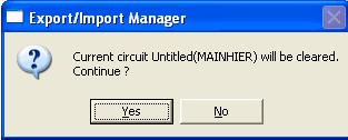
- When the Import is clicked, a message pops up as shown below. Click Yes to continue (Fig 4)
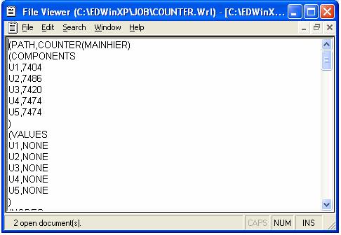
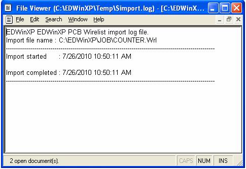
- After importing the *.wrl file, the *.wrl file as well as the import log file will be generated. These are given in the below two images (Fig 5 and Fig 6)
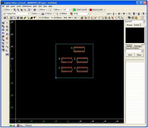
- After the import is completed, invoke Layout Editor. You can view the components are placed as per the coordinates of the components in the wrl file. This is as given below (Fig 7)
- The components can be autorouted with the Arizona Autorouterin EDWinXP.
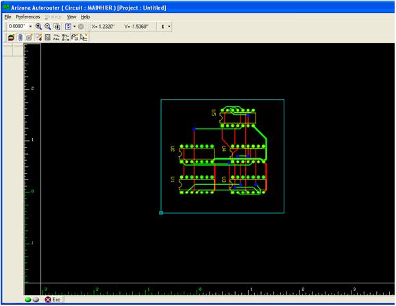
- For autorouting of the components, from Layout Editor, choose Auto -> Autorouters -> Arizona.
- Arizona Autorouter will be invoked. Choose File -> Load board to route from project. Provide the required parameters for the autorouter in the Parameter Setup functional tool.
- Then choose Auto routing routines -> Start autorouter.
- The board will be autorouted as per the parameters provided or with the default parameters of the autorouter.
- After autorouting, you can execute various tests such as Remove redundant vias, Clean up, Test for conflicts and Optimize. Finally Miter option can be executed so that the traces gets mitered.(Fig 8)
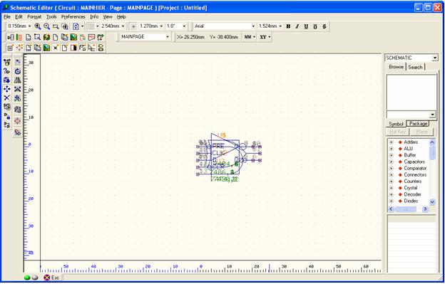
- The symbols corresponding to the layout will are generated in the Schematic Editor and will be stacked in the middle of the page. (Fig 9)
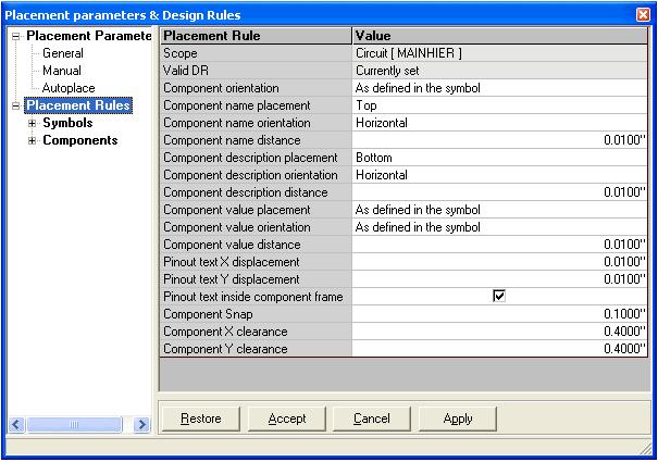
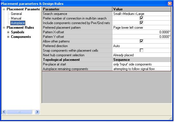
- In order to place the components in the Schematic Editor , you can autoplace the components using the Autoplace option. This function can be accessed from Tools -> Autoplace. Before autoplacing, the Placement parameters and Design rules has to be set first which can be accessed from Autoplace parameters -> Display parameters arameters and selFor that invoke display parameters and select ‘Placement Rules’ and set the parameters as given in the image below (Fig 10)
- After giving all the necessary input to the Value, click on Applybutton so that all the parameters get applied. lace and then set the values as given in the below image (Fig 11). We are following the Topological placement of components. Hence set the Sequence as given
- Pre-place at start - only ‘input’ side components
- Autoplace remaining components - attempting to follow signal flow
- Then select Autoplace all components (fifth function tool)-> Autoplace topologically
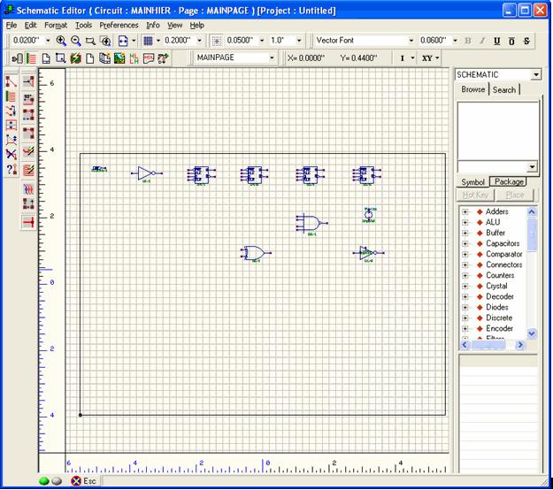
- Click on Yes to proceed with the autoplacing. (Fig12). The autoplaced components will be distributed in the schematic as shown below (fig 13).
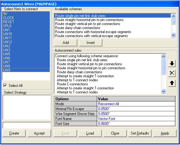
- For autorouting of the components, select Tools-> Connections -> Connect Components (first function tool) -> Autoconnect all wires (F6) (sixth option tool) (fig 14).
- Choose Select All check box to select all the nets. Then click Apply -> Close(Fig 14).
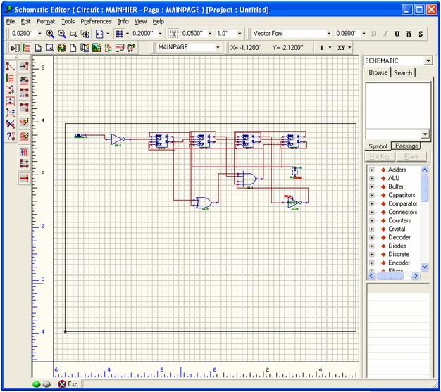
- The circuit will be autorouted as in the given image below (fig 15).
