 View Video
Implemented the efficient way to extract the List of Materials
In the List of Materials-Preview window of older versions,the same parts details were placed in different rows. In EDWinXP 2.1,the same parts details is placed in a single row along with its quantity mentioned in the "No of Components" fields. List of Materials Editor can be invoked by the following steps,
- Select EDWinXP Main → File → Open Project→ PCB Layout → Edit PCB Layout
- Click on Switch To → List of Material Editor
- List of Material Editor window appears, Select the required fields and click on next button.
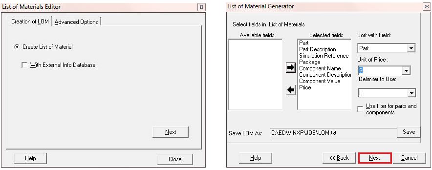
- List of Materials - Preview window appears,
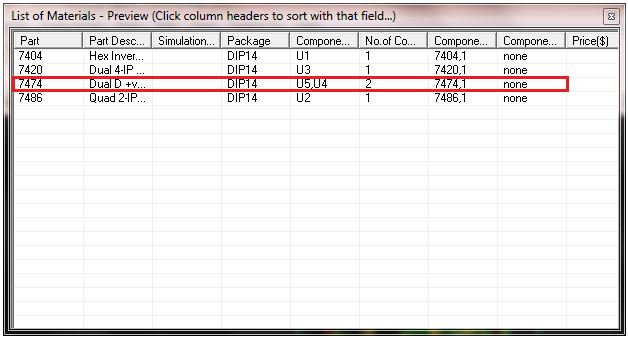
In the above window,the repeated component is shown highlighted. This will minimize preview window size.
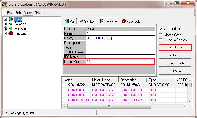
Library Browser
In Library Browser,the Packages can be searched by entering the number of pins.This option simplifies the task of searching packages of required pins.
View Video
Search packages by no of pins
- Select EDWinXP Main → Library Editor → Library Browser
- Click on the Package Browser
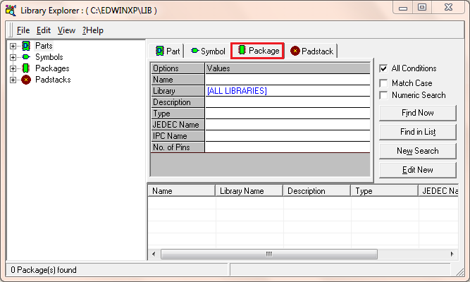
- A new option called No. of Pins is included
- Entering the No. of Pins and Clicking on Find Now button will display all the packages with the corresponding number of pins.
View Video
Library Editor
Device Cutouts Option
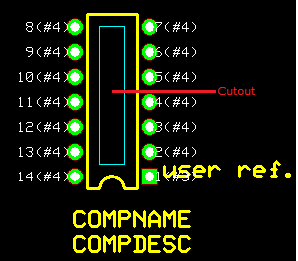
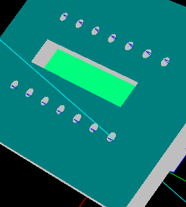
In the older versions of EDWinXP it is not possible to define milling slots in a package.In EDWinXP 2.10,the Library Editor is facilitated with the same.
Device Cutout option can be invoked by the following steps,
- Select EDWinXP Main → Library Editor → Package Editor
- Open or create the package.
- Click on the Device Cutouts option
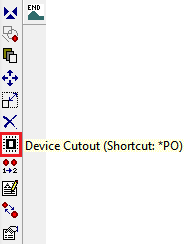
- Create the required Cutouts and click on the END tool.
The cutout created is shown in blue color in the below image.
The 3d view of the cutout is shown below.
Library Explorer
Added new library parts in Library Editor
- Select EDWinXP-Main → Library → Library Explorer
- Newly added about 7800 library parts in the new version of EDWinXP
| Manufacturers Name |
No of Components |
|
Abracon corporation
|
11
|
|
Active Semiconductor
|
52
|
|
ADESTO
|
169
|
|
ALPHA OMEGA
|
49
|
|
American Microsystems(AMIS)
|
2
|
|
Analog Devices
|
21
|
|
ATI
|
13
|
|
BKC International
|
153
|
|
Burr-Brown
|
18
|
|
DATEL
|
129
|
|
C&D TECHNOLOGIES
|
12
|
|
CADDOCK
|
41
|
|
Central Semiconductor Corp.
|
190
|
|
COMCHIP
|
31
|
|
CREE
|
132
|
|
CTS
|
18
|
|
Cypress
|
197
|
|
DC COMPONENTS CO LTD
|
45
|
|
DIODES INCORPORATED
|
61
|
|
EIC
|
108
|
|
ELMOS
|
65
|
|
EXAR
|
214
|
|
Fairchild
|
244
|
|
FASTRON
|
29
|
|
GENERAL SEMICONDUCTOR
|
37
|
|
GeneSic Semiconductor
|
8
|
|
HITTITE
|
2
|
|
Honeywell
|
12
|
|
Infineon technologies
|
14
|
|
Intersil
|
12
|
|
JGD
|
78
|
|
JIANN WA ELECTRONICS
|
1024
|
|
KAMAYA
|
100
|
|
KOA SPEER ELECTRONICS,INC
|
77
|
|
Little Demon
|
100
|
|
LITTELFUSE
|
35
|
|
MELEXIS
|
113
|
|
Micro Commercial Components
|
38
|
|
MULTICOMP
|
33
|
|
Maxim
|
347
|
|
Microchip
|
8
|
|
Microsemi
|
15
|
|
MEGATRON
|
5
|
|
micro
|
8
|
|
MPS
|
54
|
|
National Semiconductor
|
34
|
|
NTE
|
8
|
|
NXP
|
187
|
|
OHMITE
|
100
|
|
ONSEMICONDUCTOR
|
404
|
|
Philips
|
38
|
|
Power Integrations Inc
|
31
|
|
RECTRON Semiconductor
|
120
|
|
ROHM
|
24
|
|
SEMTECH
|
2
|
|
SKYWORKS
|
4
|
|
SUMIDA
|
44
|
|
SUNTAN
|
7
|
|
ST Micro Electronics
|
476
|
|
SPRAGUE
|
30
|
|
SYC
|
4
|
|
TAIWAN SEMICONDUCTOR
|
239
|
|
THAT Corporation
|
41
|
|
Texas Instruments
|
599 |
|
TDK
|
26
|
|
TE CONNECTIVITY
|
99
|
|
TOKEN
|
24
|
|
TRIQUINT
|
38
|
|
TT ELECTRONICS
|
144
|
|
UNISONIC TECHNOLOGIES C0.,LTD
|
3
|
|
Vishay
|
413
|
|
WTE
|
156
|
|
Wruth Elektronik
|
12
|
|
WEIDMULLER
|
57
|
|
YAGEO
|
100
|
View Video
Preview of components as docked view
In
Library Explorer ,a new option called
Symbol/Package Preview is added. It can be invoked by the following steps,
- Select EDWinXP-Main → Library → Library Explorer
- The preview window is shown below.
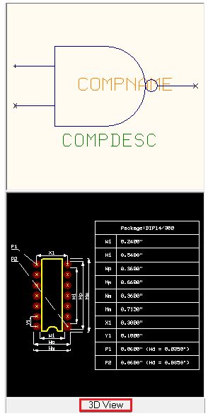
-
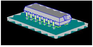
Clicking on the 3D View button will enable the 3D view of the component.
Schematic Editor
View Video
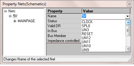
Dropdown list in Property Net Window
While editing the node name,it would be better to have a dropdown listbox from which the existing nodes can be selected.
EDWinXP 2.10 is facilitated with the same. It can be invoked by the following methods,
- Select EDWinXP Main → Open the project → Schematic Editor
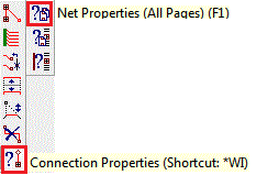
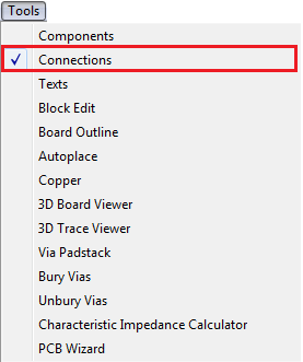
- Click on Tools → Connections
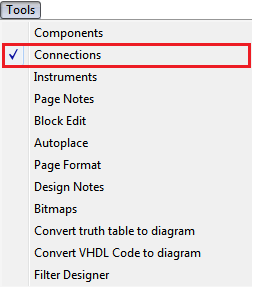
- Click on Connection Properties → Net Properties(All Pages)
- Click on the net.A Property Nets window appears.
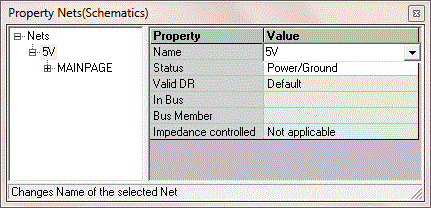
- Name and status is facilitated with drop down lists with existing nodes.This will avoid mistakes.
View Video
Net Information
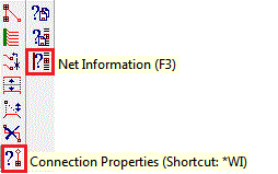
- Select EDWinXP Main → Open the project → Schematic Editor
- Click on Tools → Connections
- Click on Connection Properties → Net Information
The Schematic Editor Net Information window appears as shown below.
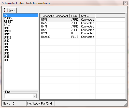
This window shows the components of each net and the status,whether they are connected or not.
View Video
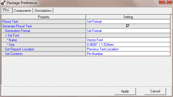
Package Preference Settings
- Select EDWinXP Main → Open the project → Schematic Editor
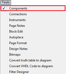
- Click on Tools → Components
- Click on Pack/Unpack Component → Package Preference
 Package Preference
 window appears
-
Change the settings as required.Click on OK
View Video
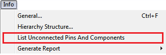
List of unused components
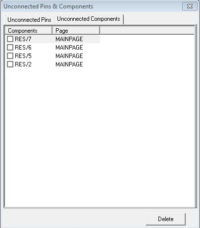
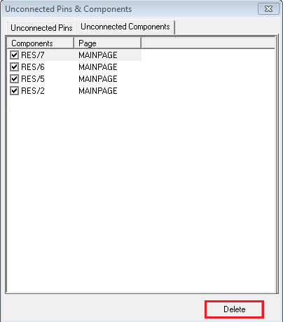
The Schematic Editor Info menu is provided with an option called List of Unconnected Pins & Components.
Invoking this option will provide the Unconnected Pins & Components window, where unconnected pins and components will be listed.
The window is facilitated with the option to select and delete the unconnected components.
The window can be invoked by the following steps,
- Select EDWinXP Main → Open the project → Schematic Editor
- Click on Info → List of Unconnected Pins & components
Unconnected Pins & Components window appears as shown below
-
The components can be selected and deleted by clicking on the delete button.
View Video
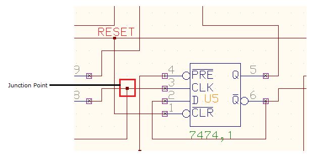
Junction Point On/Off
- Junction point indicates the merging point of 2 or more connections.
- This can be invoked by clicking on View → Schematic → Junction Point or from the Schematic View
-
Enabling this option will create junction points in the circuit where 2 or more connections meet.
Layout Editor
View Video
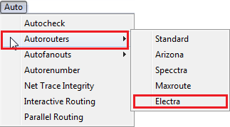
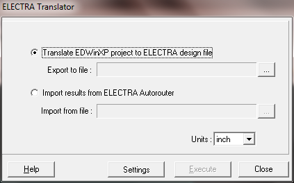
Electra Autorouter
EDWinXP 2.10 supports all
ELECTRA compatible file formats. The electra translator can export current data base to ELECTRA format design files(.dsn).
You can either use the pre set design rule settings or use new design rules while exporting the data base.
It also has the capability to import the ELECTRA Autorouters files (with extension .ses, .rte, .plc,) to EDWinXP.
- Select EDWinXP Main → PCB Layout → Edit PCB Layout
- Click on Auto → Autorouters → Electra
The Electra Translator window is shown below
View Video
Changing all the Vias of a circuit at the same time
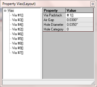
In the older versions there is no tool for changing properties of all the vias of a circuit at the same time.The new version is provided with the possibility of changing properties of all the vias at the same time.
- Select EDWinXP-Main → Open the Project → PCB Layout → Edit PCB Layout
- Click on Edit → Select All
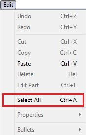
The resulting layout window is shown below.
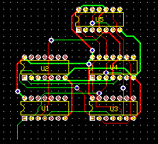
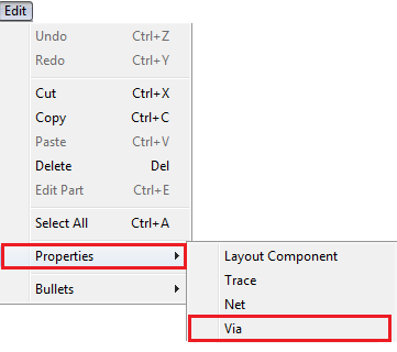
- Click on Edit → Properties → Via
A new window Property Vias appears with all the vias in the circuit
View Video
Displaying the Total Length of a Net
- Select EDWinXP Main → Open the Project → PCB Layout → Edit PCB Layout
- Click on Tools → Connections
- Click on Connection property → Net property
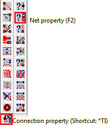
- Click on the Net
- The Property Nets Window appears as shown below
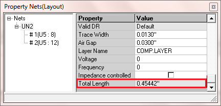
An option called
Total Length is included which shows the total length of UN2.
View Video
Jumper option for single layer routing
A Jumper is a short length of conductor used to close, open or bypass part of an electronic circuit. They are typically used to set up or configure Printed Circuit Boards.The Jumper option can be invoked by the following steps,
- Select EDWinXP-Main → PCB Layout → Edit PCB Layout
- Place the components
- Click on Tools → Connections → Route
- Route the components,move the mouse pointer to the jumper
and click on the jumper tool
 ,continue routing.
The portion after clicking the jumper tool is highlighted in the above window.The 3d view of the same is shown below.
The artwork view is shown below
Option to choose the required trace when overlapping
- Select EDWinXP Main → PCB Layout → Edit PCB Layout
- Click on Tools → Connections
- Click on the Route
 Option and route traces in the layout (wires in schematic).
When two or more traces overlap,the overlapped traces can be removed or relocated. For this choose the required option tool,click on the trace.
A popup window appears as shown below which confirms the trace.
Clicking on
YES confirms the particular trace.
View Video
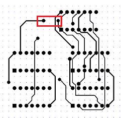
Enhanced copper pour test
In EDWinXP 2.10, on clicking the
Esc key after the copper pour flood test,the layout design of the circuit is obtained without any change rather than missing some of the connections.
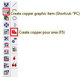
- Select EDWinXP Main → File → Open Project→ PCB Layout → Edit PCB Layout
- Select the tool Copper
- Click on Create copper graphic item → Create copper pour area
Draw the
copper pour item in the selected net
- Click on Tools → Connections
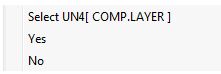
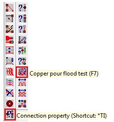
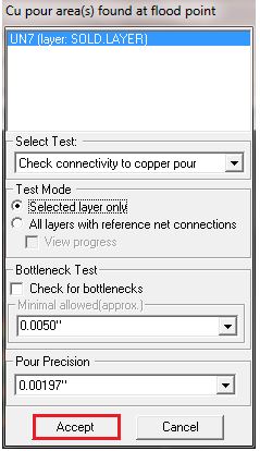
- Click on Connection Property → Copper pour flood test
-
Click on copper pour area. In the window that appears,click on Accept.
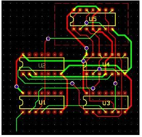
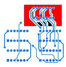
The output window is shown below.
-
Clicking Esc key will provide the original layout design of the circuit rather than missing some of the connections.
View Video
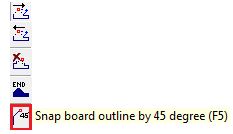
Snap board outline by 45 degree
A new option called
snap board outline by 45 degree is included in the PCB Layout Editor. This option may be used to define outline with 45° angular snap. The outline can be defined to different directions only in steps of 45°.
-
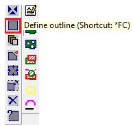
Select EDWinXP-Main → PCB Layout → Edit PCB Layout
- Click on Tools → Board Outline
- Click on Define outline
-
Select this function tool. On enabling the option snap board outline by 45 degree, the angular steps allowed for defining outline to different directions will only be 45°.
View Video
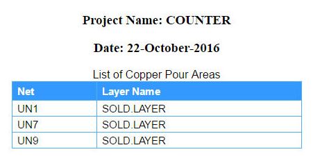
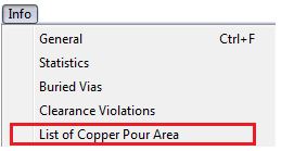
List of Copper pour Areas
-
List of Copper pour Areas in Layout Editor is an additional feature. This option can be invoked from the Info menu.
-
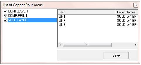
A window will appear that contains the list of copper pour areas in the circuit.
-
Click on Save button.Save the list of copper pour areas as html files.