New features from EDWinXP ver 1.30 to EDWinXP 1.50
New Features of EDWinXP 1.30 and EDWinXP 1.40 clubbed together – What’s New
Schematic Editor
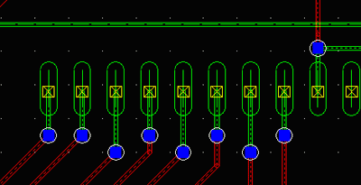
1. New Autoplacer tools:
In Tools | Autoplace
. Group by category: This function tool along with a set of option tools may be used to group components together in the bins based on certain criteria like nature of, nature of connections or nature of terminals.
Option Tools include:
- Include already placed: Option to include already placed components in the category group.
- Group 'Input' components: Groups components which are connected to input nets for the page. The components with single nodes on the left side are detected by the autoplacer as input nets.
- Group 'Output' components: Groups components, which are connected, to output nets for the page. The components with single nodes on the right side are detected by the autoplacer as output nets.
- Group by bus: Groups components connected to a bus and places them in the Component Groups Bin.
- Group by net: Groups components connected to a net and places them in the Component Groups Bin.
- Group 'Input' terminals: Option to group components recognized as 'input-to-page' terminals.
- Group 'Output' terminals: Option to group components recognized as 'output-from-page' terminals.
- Group 'Inside' components: Option to group all the components, which are not included in the input or output category.
- Append group: Enables groups of different categories to be accomodated in the Component Groups Bin at the same time.
- Relocate Component: Tool to relocate component/ component text. Options may be used to rotate by 90°, any angle, change the placement side, relocate component with name specified, swap components placement, toggle display of ratsnest/ trace/ outline etc.
- Relocate Block: Tool to relocate selected block to another position. Its set of options may be used to rotate the block by 90°, any angle, and to relocate items in the block including the page outline.
- Reroute Connections: Tool to autoroute wires while carrying out Manual / Autoplacement. This tool has been provided for convenience so that the user does not have to take the trouble of switching to Tools | Wires & Buses to start routing the connections.
- Net Property and Component Property: Tool to view/change properties of selected net and/or component.
In Tools | Autoplace | Autoplace all components
1. Autoplace Topologically: Option tool to place components automatically based on circuit topology.
2. Instant Packaging
This new menu item under Preferences menu in Schematic Editor helps to pack components as soon as they are loaded to the workspace. All the constituent groups of the part will be loaded. This is particularly useful while loading connectors into the Schematic.
3. Autocovering
Auto covering avoids switching between the tools. Option tools delete, properties and relocate are now common in all the function tools. In order to avoid confusion between nets and traces a common tool named connections is introduced in which the nodes option has also been included.
4. Component Browser
Customizable component browser has been introduced in Schematic Editor. The browser embedded in Schematic Editor provides the facility to browse and search for components.
5.Block Diagram Elements
This feature allows for simplified creation of block diagrams of hierarchical circuits. There is no longer need to create block diagram elements using Library Editor since part descriptions and symbols are automatically created according to user’s specification. Nevertheless, parts and symbols created for block diagram elements may be edited like any other library element and stored in the disk libraries for farther use.
6. Component Specific MM Simulator Models
Mixed Mode simulation models may be assigned individually to components, hence overriding current model assignment to symbols. Component specific simulation models may be assigned to block diagram elements.
7. Truth Table to diagram converter
Logic function defined in form of truth tables may be converted to equivalent schematic diagram that may be later attached to currently edited page, form a new page in edited circuit or be attached as new circuit in the project.
8. Direct assignment of logic function to schematic components
Logic function of selected schematic component may be specified either through truth table or VHDL code and attached in form of hierarchical sub-circuit or automatically generated simulation model. Generation of both MM Simulator and EDSpice code models is supported.
9. VHDL Code Converter
This function enables conversion of VHDL code into schematic diagram.
10. Vertically or horizontally oriented net/bus page link notes
Depending on user’s preference, net/bus page link notes may be generated either as vertical or horizontal bar. Vertical bar was the only option in previous versions.
Mixed Mode Simulator & EDSpice Simulator
1. Model Interface
Model Interface is a centralized management tool, used for configuration of any kind of either analog or digital component of Mixed-mode Simulator. It allows the simultaneous administration of different components on the model level.
2. Transient Analysis - Logic Analyzer:
Now it is possible to directly launch the Logic Analyzer from the simulator window. A user may use this dialog to get the textual values for digital (binary, octal, hexadecimal and decimal) and analog waveforms at different test points.
3. Multichannel display in Oscillograph:
Option to view four channels in their respective axes simultaneously.
4. EDSpice Interactive Interpreter:
EDSpice Interactive Interpreter has been revamped to include features to directly initiate simulation from .cir file. Apart from this, it also incorporates features for creating new, editing and saving existing .cir files.
5. Simulators embedded in Schematic Editor
Both Mixed Mode and EDSpice Simulators are now incorporated in Schematic Editor, thus avoiding the need to switch between the modules.
6. Circuit File Editor
Circuit File Editor is used for editing SPICE circuit file and running simulation. The circuit file (.CIR file) describes the circuitry to be analyzed in a format that the SPICE simulation engine can interpret.
7. Instant Probes
These probes are used for instant display of transient analysis result of desired nets/nodes in an analog/digital circuit.
8. 8051 Microcontroller Kit
The kit contains new simulation model of microcontrollers of 8051 family and application examples. The 8051 model uses MMI technology that enables edition and compilation of programs in C-language and assembler, debugging the code and simulation together with whole circuit. Attached simulation examples help in evaluating the kit and learning how to use the model for the development of microcontroller programs. The kit contains also series of so called instrumental model for generating parallel and serial binary data patterns and asynchronous hardware interrupts. Usage of 8051 model in user’s designs requires separate license.
This kit includes example project databases designed to illustrate functionality of the new simulation model for 8051 microcontrollers. Each project comes with associated help file that explains the example in details. The latest software version of the model is included as well as 8051 code C compiler and function libraries. The new MMI model for 8051 allows coding programs in C or Assembler and debugging them in real time while functioning of the rest of circuitry is simulated. To facilitate analysis of more complex microcontroller based circuits, the kit includes also several instrumental MMI models such as memories, interrupt generators, serial/parallel pattern generators, 7-segment displays etc. The Multifunction Model Interface (MMI) dialog for 8051 model supports following features:
• C Editor
• Assembly Editor
• Listing View
• Hex Editor
• Disassembler
• Output File
• Errors and Warnings
9. PIC Microcontroller Kit
The PIC kit includes main projects with assembler source code, which illustrates the functionality of PIC microcontrollers, with associated help files The latest software version includes the PIC model and it's function libraries. The new MMI model for PIC allows coding in Assembler Editor and debugging them in real time while simulating with the rest of circuitry. To facilitate analysis of more complex microcontroller based circuits, the kit also includes, several instrumental MMI models such as serial/parallel pattern generators, interrupt generators, 7-segment displays etc.
The PIC16C5x is the current version included in EDWinXP.
The Multifunction Model Interface (MMI) dialog for PIC model supports following features:
• Assembly Editor
• Listing View
• Hex Editor
• Disassembler
• Output File
• Errors and Warnings
10. AVR Microcontroller Kit This kit includes example project databases designed to illustrate functionality of the simulation model for AVR AT90S2313 Microcontroller. Each project comes with associated help file that explains the example in details. The new MMI model for AVR AT90S2313 allows coding programs in C or Assembler and debugging them in real time while functioning of the rest of circuitry is simulated.
Users can design complex microcontroller based circuits with the use of instrumental MMI models such as memories, interrupt generators, serial/parallel pattern generators, 7-segment displays etc.
The Multifunction Model Interface (MMI) dialog for AVR AT90S2313 Model includes the following modules:
• C Editor
• Assembly Editor
• Listing View
• Hex Editor (ROM)
• Hex Editor (EEPROM)
• Disassembler
• Output File
• Errors and Warnings
MM Simulation Model Generator
1.Analog Model TypeMM Simulation Model Generator enables to generate models of analog circuit elements. The logic function of analog elements may be very precisely described in so-called SPICE netlist format. Therefore the source for analog model generation is ASCII file containing SPICE sub-circuit.
PCB Layout Editor
1.New Autoplacer tools:
In Tools | Autoplace
Ø Relocate Component: Tool to relocate a component/ component text/ testpoints. There are options to rotate through 90 °, any angle, change the placement side, relocate component with name specified, swap components placement, toggle display of ratsnest/ trace/ outline etc. This tool is defined in Tools | Components but has been included with the Autoplace tools for convenience.
Ø Relocate Block: Tool to relocate items selected in a block. There are options to rotate the block through 90°, through any angle, and to relocate items in the block including the board outline. This tool is defined in Tools | Block Edit but has been included with the Autoplace tools for convenience.
Ø Component and Net Property: Tool to view/change properties of selected component/component name, selected net, view a selected net on the Layout with its properties and to view the Schematic info of a selected net.
2. Component Browser
Customizable component browser has been introduced in Layout Editor. The browser embedded in Layout Editor provides the facility to browse and search for components.
3. Meshed Copper Pour Areas Display
This tool enables to view the meshed copper pour areas on a particular layer in the layout.
4. Multilayer copper pour connectivity check with 3D presentation included
Copper pour connectivity check, working in similar way as in Fabrication Manager, has been added to PCB Layout Editor. 3D presentation may be used to visualize detected errors on all layers where tested net connections are located.
5. Improved presentation of copper pours
On request, coppers pour areas may be presented filled by meshed pattern for better visualization of boundaries on densely packed PCB layouts.
6. Auto Connect Functions
Auto-connect tools in Layout Editor are complement to manual trace routing tools. These auto-connect functions work directly on items in the project database. Execution time depends very much on the complexity of the board. Whether routing task is completed successfully depends on topology of currently existing connections.
The new Auto connect tools come under Tools | Connections | Auto Connect Traces are:
Ø Auto Connect Node Pair : Routing connection from node to node.
Ø Auto Connect Net: Routing connections for all nodes in selected net with the option to keep pre-routed traces unaltered.
Ø Auto Connect Net Element: Routing connection from selected net element (existing trace or node) to closest located element in the same net.
Ø Auto Lead-Out from Net Element: Routing lead-out traces from component nodes.
Ø Auto Clear Component Zone: Clearing a zone around a component(s) and re-routing all traces not connected to this component outside of the zone boundaries.
Ø Auto Remove Vias: Removing redundant via holes on the whole board.
Ø Auto Miter: Mitering all traces on the board in 45 degrees.
Fabrication Manager
1.Improved multilayer copper pour connectivity check with 3D presentation
Previously implemented copper pour connectivity check has been enhanced for simultaneous testing of all artwork layers where connections for selected net are present. User may examine location of detected unconnected or isolated pads and isolated via holes with help of two or three dimensional presentation.
2.Polygonal copper relieve
Definition of areas on the artwork where copper should be removed from copper poured Gnd/Power planes was previously done through placing items like rectangles and circles. In present version relieve areas may be defined by polygons. A feature useful for removing of isolated islands of copper that usually have irregular shapes.
3. 3D export in IDF format
Feature allowing for exporting 3D view of the PCB in IDF Ver. 3 format
4.3D IDF file viewer
Three-dimensional presentations of IDF Ver 3 format files.
Copper Removal Tools
5. Automatic Copper Cleanup
Enables removal of all "black" copper areas (isolated areas) from the artwork. The program analyses display of the artwork after test and generates copper relieve items in number and sizes necessary to cover all detected black spots.
6. Semi - automatic copper trimming
Enables to trim isolated "black" copper or connected "red" copper on the board. Trimming is necessary, especially when there are areas of connected (red) copper that are superfluous.
7. Polygonal Copper Relieve
Enables removal of isolated islands of copper that usually have irregular shapes (polygonal shape).
Library Editor
1. Triangular Package and PadstackAllows to create triangular package and padstack.
3D Graphics
1. User definable true colorsApart from 32 standard colors, the user may define custom palette of 224 colors and assign them to objects in three-dimensional visualization.
2. Improved scrolling and navigating
Current scroll position is retained when switching between 2D and 3D presentation. This is useful for examining results of connectivity check where alternating views without losing focus on the object is often required. Rotation of 3D view is executed around currently focused location rather then around coordinate system origin.
3. Semi-transparent view of copper pour areas and layout components
An extremely useful feature for 3D visualization of multi layered PCB designs.
General
1. Text Formatting:
Additional text formatting feature has been included in the Edit & Add Text Block dialog of Schematic Editor and Library Editor. This feature allows to add text of type Vector Font with an overline. e.g .
2. Import / Export Utilities:
This version of EDWinXP’s Netlist/Wirelist Import and Export utility allows to import / export ALTERA EDF files to / from EDWin. It is also possible to convert EDWin Schematic Netlist to ALTERA EDF format and vice-versa.
Following release of previous version, several new features and improvement to existing features have been implemented in EDWinXP 1.50
PCB Layout Design and Fabrication
1. Copper pour connectivity test have been added PCB Layout Editor. Similar test was already included in Fabrication Manager. The advantage of this test in Layout Editor is that the connectivity may be checked while the board layout is designed. In both modules, the test may be now performed in selectable accuracy of 0.100, 0.050 and 0.025 mm. The time needed to execute the connectivity test has very significantly reduced.
2. Polygon shapes for copper removal introduced in 1.40, allowed to add feature that automatically removes unnecessary copper in isolated places within copper pour areas. This function was available for 1.40 users through live update. In 1.50, it has been improved in both speed (about 50% reduction of execution time) and accuracy.
3. Gerber View feature has been improved in order to reduce number of selections necessary to pre-process and display artworks in Gerber formats.
4. The option to plot inverted polarity circles and squares in size of pinholes for PMD component and vias has been added for Gerber format output. This option is available for in RS-274-X format only.
5. Settings for all fabrication exports (GenCAM, IDF and newly added Valor’s ODB++ format) have been grouped in common dialog within Fabrication Manager.
6. It is now possible to import projects from other EDA packages in ODB++ format
7. Reconstruction of projects from Gerber format artworks been have significantly improved by adding feature for rebuilding component parts and packages from imported graphics. Projects can be now completely reconstructed even if necessary library elements are not available.
8. Number of tools for automatic routing of connection in PCB Layout Editor has been increased. It is now possible to automatically connect two separate trace branches of a net, re-route connections for a group of relocated components, route lead-out traces from pins of component with complicated pad patterns, automatically miter traces and remove redundant via holes.
9. Online clearance check has been introduced with improved visibility for detected clearance violations.
10. It is now possible to display ratsnest in two modes: will all nodes or with unconnected nodes only.
11. Important function “re-route” trace may be now performed in two modes: “re-route trace segment” and “re-route pin to pin connection. This latter is particularly useful when cleaning up design after auto-routing.
12. Node marker size (squares) and pin entry marker size (crosses) are automatically adjusted to the pitch of component pads in order to ensure best visibility. Similarly, via hole marker size is automatically adjusted to smallest hole diameter in via pad stacks
Schematic Capture and Simulation
1. New feature called Filter Designer has been added. The system library includes prototype circuits for active low-pass, high-pass, band-pass and band-stop filters. Filter Designer allows to select one of the variants of those filters (Chebyshev, Butterworth, Bessel, Elliptic (Cauer) or Universal) and specify required filter output parameters – frequency and quality range. The parameters (capacitance and resistance) for filter circuit components are calculated and updated in the circuit, which subsequently may be appended to the project.
2. It is now possible to convert functional descriptions of discrete parts, expressed in form of SPICE format sub-circuit into analogue model for Mixed Mode Simulator.
3. Following code models have been added to MM Simulator and EDSPice model libraries:
4. New feature called Filter Designer has been added. The system library includes prototype circuits for active low-pass, high-pass, band-pass and band-stop filters. Filter Designer allows to select one of the variants of those filters (Chebyshev, Butterworth, Bessel, Elliptic (Cauer) or Universal) and specify required filter output parameters – frequency and quality range. The parameters (capacitance and resistance) for filter circuit components are calculated and updated in the circuit, which subsequently may be appended to the project.
5. It is now possible to convert functional descriptions of discrete parts, expressed in form of SPICE format sub-circuit into analogue model for Mixed Mode Simulator.
6. Following code models have been added to MM Simulator and EDSPice model libraries:
EDSPICE code models MM Simulator models
M7218CD DAC0800
Max456 ADC0800
Max4587 MAX232
Max522 DAC AD 569
max5341 HPDL1414
max5352 ULN2003A
max625 Stepper Motor
max690 Potentiometer
max691 LCD Display
max696 LCD Display Driver-HD44780U
max697 SweepGenerator.dll
max701
max702
max708
max7225
MAX7240
7. EDSPICE updates for EDWinXP 1.50
Sub-circuit files
• Diac
• CCCS
• CCVS
Circuit files (SPICE netlist format)
• BUCK CONVERTER AC MODEL.CIR
• DC_MOTOR_MODEL.CIR
• TREBLE AND BASS TONE CONTROLS.CIR
• I-TO-V CONVERTER (TRANSIMPEDANCE AMP).CIR
• CCCS.CIR
Sample projects with new EDSPICE sub-circuits
• 7805 Regulator - voltage regulator 7805
• CENTRE TAPPED TRANSFORMER - transformer
• Controlled Full Wave Rectifier - SCR
• OPTOCOUPLER- OPTOCOUPLER
• IGBT - IGBT
• Sidac characteristics - sidac
• UJT Relaxation Oscillator – UJT
• Current Controlled Current Source - CCCS
• Current Controlled Voltage Source – CCVS
Updates in Part Libraries
| PART | MANUFACTURER | SYMBOL | PACKAGE |
| 0805AS-2N7M-01 | Fastron | INDUCTOR | L/L70/SM |
| 59S101-400E3 | Rosenberger | CONN | CON/F5/A |
| 74HC4052D | Philips | MUX4052 | SOIC16/150 |
| 8516-4500 | 3M Interconnect Solutions | CONN | CON/HEADER16/A |
| 8520-4500 | 3M Interconnect Solutions Division | CONN | CON/HEADER16/A |
| 8526-4500 | 3M Interconnect Solutions Division | CONN | CON/HEADER16/A |
| 8540-4500 | 3M Interconnect Solutions Division | CONN | CON/HEADER16/A |
| 8560-4500 | 3M Interconnect Solutions Division | CONN | CON/HEADER16/A |
| A3953SB | Allegro | DRV3953 | DIP16/300 |
| ACSL-6400-T | Agilent Technologies | OPTO6400 | SOIC16/150 |
| ADF7020BCPZ1 | Analog Devices | TxRx7020 | LCC48/A |
| AT91SAM7S64 | Atmel | MICR91SAM7S | QFP64/D |
| ATmega128L-8MC | Atmel | MICR128 | LCC64 |
| bq24022DRC | Texas Instruments | ADPTR24022 | LCC10 |
| BSP742T | Infineon technologies | SWT742 | SOP8/150 |
| C-551SR | Para Light | DISP5503 | DIP10/600 |
| CY8C27443-24PXI | Cypress | MCNTRLR8C27443 | DIP28/300 |
| DB15SRT/3R | Amphenol | CONN | CON/DB15/D |
| DCP010515DBP-U | Burr-Brown | DCP0105D | DIP14/300/P7 |
| DS1822 | Dallas Semiconductor | THERMO1822 | TO92/3 |
| dsPIC30F5011 | Microchip | CNTRLR30F5011 | QFP64/C |
| dsPIC30F6011 | Microchip | CNTRLR30F6011 | QFP64/C |
| dsPIC30F6014 | Microchip | CNTRLR30F6014 | QFP80/B |
| EP2C8F256 | Altera | FPGA8C256F | BGA256/e40 |
| F3345 | FOX Electronics | XTALOSC1 | DIP4/SM/3 |
| FDC6301N | Fairchild | PFET_DG | SOT23/6 |
| FDV303N | Fairchild | NFET_DG | SOT23/3 |
| FSA4157P6 | Fairchild | SPDT4157 | SC88 |
| G5V-2 | OMRON | RLY1FORMC,RLY1FORM | DIP16R/8 |
| GM5WA06260A | SHARP | LED | DIP6/SM |
| L5973D | ST Micro Electronics | VREG5973 | SOP8/150 |
| L6203 | ST Micro Electronics | DRV6203 | TO220/11 |
| LAN91C111 | SMSC | LAN91C111 | QFP128/C |
| LATBT66C | OSRAM | 3DIODE | DIP4/SM/B |
| LPC2106FBD48 | Philips | MCNTLR2106 | QFP48 |
| LZ-12VM | FUJITSU | RLY1FORMC | DIP5 |
| M54562FP | Mitsubishi | DARARRAY54562 | SOP20/200/A |
| MAX5400EKA-T | Maxim | DPOT5400 | SOT23/8 |
| MAX952ESA | Maxim | AMPR952 | SOIC8/150 |
| MC6802P | Motorola | MICR6802 | DIP40/600 |
| MC6821P | Motorola | ADAPTR6821 | DIP40/600 |
| MCF5235CVM100 | Freescale | MICR5235 | BGA256/e40 |
| MIC2941ABU | Micrel | VREG2941 | TO263/5 |
| MM5450BN | Micrel | DRV5450 | DIP40/600 |
| MMA7260Q | Freescale | ACCLR7260 | QFN16 |
| MSC1202Y2RHHR | Texas Instruments | ADC1202 | LCC36/A |
| nRF905-EVKIT 868/915 | NORDIC | TxRx905 | LCC32/A |
| PIC16F688I/SN | Microchip | MCNTLR16F688 | SOIC14/150 |
| PIC16F876/SO | Microchip | MICR16F873 | SOIC28/300 |
| PIC18F4220-I/P | Microchip | MCNTRLR18F4220 | DIP40/600 |
| PIC18F452-I/P | Microchip | MCNTLR18F442 | DIP40/600 |
| PIC18F452-I/PT | Microchip | MCNTLR18F442 | QFP44/C |
| PIC18F4550 | Microchip | MCNTRLR18F4550 | DIP40/600 |
| PIC18F458-E/L | Microchip | MCNTRLR18F458 | LCC44 |
| QMB-111PC | Star | BUZZER | PMD2/e12 |
| QT1080-ISG | Quantum | SENSOR1080 | LCC32/A |
| RY-12 | FUJITSU | RLY1FORMC,RLY1FORM | DIP16R/8 |
| TA7252AP | Toshiba | AMP7252 | SIP7/A |
| TDA7294V | ST Micro Electronics | AMP7295 | TO220/15 |
| TEL3-2422 | Traco | CONV2422 | DIP14/400/8 |
| TLE5205-2GP | Infineon technologies | BRIDGE5205 | SOP20/425 |
| TLE6228GP | Infineon technologies | SWT6228 | SOP20/425 |
| TLE6232GP | Infineon technologies | SWT6232 | SOP36/400 |
| TLMK330 | Vishay | LED | LCC2 |
| TMP36FS | Analog Devices | SESOR36 | SOIC8/150 |
| UC3906DW | Texas Instruments | ADPTR3906 | SOIC16/300 |
| ULN2004D | ST Micro Electronics | DARARRAY2003 | SOIC16/150 |
| XC9572 | Xilinx | PLD9572 | LCC44 |
| TJA1040 | PHILIPS | CANCNTR1040 | SOIC8/150 |
| LM317AMDT | NATIONAL | ADVOLTREG | TO252/C |
| FT232RL | FTDI Chip | UART232A | SOP28/200 |
| 2SA933AS | Rohm | PNP | TO202/3/B |
| 2SC174S | Rohm | NPN | TO202/3/B |
| HD44780UA00TF | HITACHI | DISPCNTRLR44780 | TQFP80 |
| HD44780UA02TF | HITACHI | DISPCNTRLR44780 | TQFP80 |
Symbol only parts
| Part Name | Symbol |
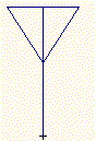
| ANTENNA |
|
| BUZZER |
|
| CAVITYRESONATOR |
|
| CIRCUITBREAKER |
|
| COAXIALJACK |
|
| CRO |
|
| EARPHONE |
|
| GALVANOMETER |
|
| GUNNDIODE |
|
| LAMP |
|
| LASERDIODE |
|
| LDR |
|
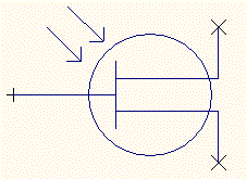
| MICROPHONE |
|
| MOTOR |
|
| OHMMETER |
|
| PHONEJACK |
|
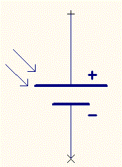
| PHOTODIODE |
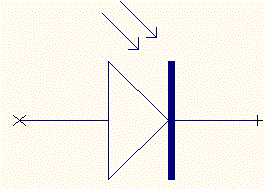
|
| PHOTOFET |
|
| PHOTOVOLTAICCELL |
|
| SCHOKELYDIODE |
|
| STEPPERMOTOR |
|
| THERMOCOUPLE |
|
| TRIMMERCAPACITOR |
|
| TUNNELDIODE |
|
| VARACTORDIODE |
|
| VARIABLECOIL |
|
| WATTMETER |
|
What is New in EDWinXP 1.60 and EDWinXP 1.61
Project Version Control
Project version control enables storing of different versions of a project in the same disk file. Current version may be saved at any time and all saved versions become part of the same project database. Any saved version may be restored immediately and set as current. Since all recorded versions are included in the same database and are loaded from and stored in a single common disk file, there is no need to keep track of different version files and worrying about backups. It would be enough to back up only one file containing all recorded versions. It also allows to reconstruct single project database with several versions that were stored as separate database files (.epb) in previous versions of EDWinXP. There are provisions to view general and statistics information’s and also to compare selected version with the active version. The new structure of database makes it incompatible with previous version of EDWinXP. Older project are fully upward compatible, can be loaded and will be automatically converted to the new format. There is also possibility to save selected project versions in a separate file in the format accepted by older releases of EDWinXP. Note: This feature is available only for EDWinXP Professional.
Layout Editor
Trace Length and Width TrimmingThis feature allows inserting pattern of segments into selected trace in order to obtain exact specified length. The shape of the pattern, its amplitude and step length may be set as parameters for calculation of necessary number of steps. All user has to do is to select the suitable point in the trace where the pattern should be inserted. This is done interactively – the pattern (generated according to currently set parameters) is visible and follows cursor while it is moved along the trace. Parameters may be adjusted during this time until permanent insertion is confirmed by the mouse click.
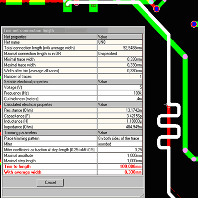 Trimming function works in three modes: trimming single trace to specified length, trimming two traces to the length of longer one and trimming net connection to specified length. In the latter mode, it is possible to see how changing of length and average trace width affects net’s electrical properties (resistance, capacitance, inductance and impedance)
As further requested improvement, the current trace length is dynamically calculated while trace is manually routed or re-routed.
Trimming function works in three modes: trimming single trace to specified length, trimming two traces to the length of longer one and trimming net connection to specified length. In the latter mode, it is possible to see how changing of length and average trace width affects net’s electrical properties (resistance, capacitance, inductance and impedance)
As further requested improvement, the current trace length is dynamically calculated while trace is manually routed or re-routed.
Automatic correction of selected clearance errors
Reporting of clearance errors have been improved by providing additional details of detected conflicts. The dialog presenting locations of conflicts is always visible (modal) while navigating from error to error. Focused errors are distinctly marked for exact identification.
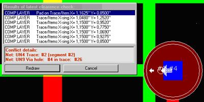 Another new feature is automatic correction of selected clearance error. This function works in two modes. Error to correct may be selected by pointing corresponding marker on the screen. The program is now able to recognize exactly which traces are in conflict. The one that creates most conflicts is automatically rerouted. In other mode, the user may select any of conflicting traces and order its automatic rerouting.
Automatic clearance correction after routing and rerouting
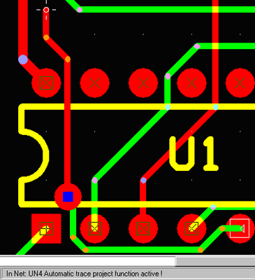
In version 1.61, the on-line clearance check feature has been strongly enhanced by automatic correction of all clearance errors caused by the last route or reroute operation. This function has several options. It may be specified that correction should be executed always when error are detected without asking. Alternatively, information that errors have been detected is displayed awaiting confirmation for executing correction. It is also possible to order that correction should apply to the last routed/rerouted trace or that this trace must be left unchanged and only other conflicting traces should be automatically rerouted.Automatic “trace project” feature
Pressing key combination, Shift A when a trace is manually routed or rerouted activates and deactivates automatic “trace project” function. Following happens, depending on currently executed operation:- When a new trace is created and the function is ON, the program automatically routes clearance error free connection from the last inserted point to current cursor position. Cursor movement changes this so-called “trace project” to reroute dynamically depending on obstacles encountered on the way. Mouse click confirms that trace project to this point is accepted and subsequent trace project starts to be routed from this point. Even if the route suggested by trace project is not accepted, the feature may be used to seek best way for manual routing. It is possible to alternate (by Shift A) between the modes and route some parts of the trace manually and some parts automatically.
- When a trace point or segment is relocated, and the automatic trace project function is ON, the program reroutes preceding and following segments of the trace, starting in both directions from current cursor position. Using option “rip-up before reroute” allows in this case rerouting of entire connection between two nodes
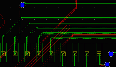
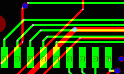 The transparency due to “XORed” trace display is clearly visible on the picture above showing True Size mode view. Trace Frames mode produces in this case small reddish circles representing position of bending points. This feature helps in detecting redundant bending points (inserted often by careless manual routing) that create unnecessary collinear trace segments
According to the same rule, oval pads created from lines of certain length and with are presented in contoured form that allows seeing their real size outlines in Centerline view mode with Pad Frames ON.
The transparency due to “XORed” trace display is clearly visible on the picture above showing True Size mode view. Trace Frames mode produces in this case small reddish circles representing position of bending points. This feature helps in detecting redundant bending points (inserted often by careless manual routing) that create unnecessary collinear trace segments
According to the same rule, oval pads created from lines of certain length and with are presented in contoured form that allows seeing their real size outlines in Centerline view mode with Pad Frames ON.
 On users’ request, Padstack Creation Wizard has been equipped with possibility to create rectangular SMD pads with rounded corners). Other issue connected to padstacks that has been solved in this version is the possibility to create SMD pads on top and bottom layers. Check for connectivity in Layout Editor that did not allow connection of trace to bottom placed pad in a component placed on top layer has been accordingly changed. This especially makes creating of packages representing finger connectors easier and more straightforward.
Shortcut to copper check added to flood test in Layout Editor
The flood test for copper pour connectivity that has been implemented in previous version has been enhanced to include also shortcut check. In this manner, all layout design testing functions are finally grouped in one application.More padstacks for via holes
Number of available padstacks for via holes (previously 7) has been increased to 16. To facilitate differentiation among various padstacks, it is now possible to add labels to each of them for individual recognition. It is even possible to highlight vias using given type of padstack.Library Editor
Auto dimensioning of packages and padstacks
Users who produce boards on order often need to document library elements created for each design, even in printed form. For this purpose, dimensioning of packages and padstacks has been implanted in version 1.61. Tables with dimensioning data in following form are created fully automatically after switching to this mode while editing packages in Library Editor or viewing them in Package Viewer: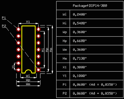
List of Material Editor
This module has been replaced by completely rewritten new version that on one hand allows creating simple lists much easier and on the other allows using advanced feature of External Info Database in more straight forward, intuitive way. Additionally, output filters have been introduced enabling to generate variants of BOMs from the same project database.Fabrication Manager
- Undo/Redo feature is implemented, which is especially needed when reconstructing projects from graphic imports.
- Introduced simple means for aligning images.
- New fabrication export has been implemented, this time for exporting CNC data in G-CODE format containing generic machining program for cutting board outline contours and internal cutouts. Toolpath for cutting are also calculated allowing for specified cutter diameter (cutting outside outer contour and cutting inside internal outlines).
Mixed Mode Simulator
As a complement to previously released development kit for PIC16C family of microcontrollers, with 1.61 we are releasing similar kit for PIC16F84/C84 family containing C-compiler, Assembler, Debugger and instructive application examples. New microcontroller kit and simulation models- New models created in MMI technology for:
- Line 5 x 8 dots LCD display full version
- HD44780U LCD display driver full version
- Line 5 x 8 dots LCD display
- Line 5 x 10 dots LCD display
- Voltmeter (instrumental)
- GLED
- OrLED
- Standard digital models:
- 74F579-8-bit bidirectional binary counter (3-State)
- 74F597-8-bit shift register with input flip-flops
Mouse wheel
Support for mouse wheel has been fully implemented in version 1.60. The wheel is used for zooming graphic display in and out with simultaneous panning to point shown by the cursor. Mouse wheel may be also used to scrolling up and down the tables (grid control) that are displayed in pop up dialogsVista compatible help system
All help files have been converted and re-edited for compatibility with Microsoft Vista operating systemMany small improvements
Many requested small improvements have been added to the system and not all of them are clearly visible. Just to mention a few:- ALT key to initiate entering of shortcut commands. This has been added for improved ergonomics.
- Provision to see total design time in project properties.
- Long cursor feature in wave form viewer.
- List of recently opened projects has been increased to 8 in project explorer's File option.
- Content of data created by List Generator program has been extended to include component values.
- Measurement function recognizes more object types (board outline) and displays not only distance but also delta X and delta Y between measured objects.
- Nodes in Net Property dialog (Schematics Editor) are displayed grouped by schematic pages where they are located.
- Pins numbers in Component Property (Layout Editor) dialog are displayed with corresponding schematic entry names
- Refreshing of elements in Project Library may be done selectively.
- Opening of padstack editor may be done directly from Layout Editor.
- Number of groups that can be added at a time is increased to 128.
LIST OF NEW PARTS UPDATED IN EDWINXP 1.61
| No. | PART | SYMBOL | PACKAGE |
| 1. | 10MQ100N | DIODE | DO214AA/2/L175/B |
| 2. | 1-1740194-2 | CONN | CON/DB9/SMD |
| 3. | 1N4148 | DIODE | SOD80/2/L125/A |
| 4. | 3296W-1-103LF | RESPOT3296 | RTP3 |
| 5. | 4HEADERL/A | CONN | CON/HEADER4/A |
| 6. | 500075-1517 | 500075-1517 | 500075-1517 |
| 7. | 8279 | I8279 | DIP40/600 |
| 8. | A3984SLP-T | DRV3984 | SOP24/170 |
| 9. | A4983SET-T | DRV4983 | LCC28/C |
| 10. | AMP 1-6605834-1 | CONNRJ10 | CON/RJ45-10 |
| 11. | ATmega1281V-8MU | MICR1281 | LCC64 |
| 12. | ATmega128L-8MC | MICR128 | LCC64 |
| 13. | ATmega64L-8MC | MICR128 | LCC64 |
| 14. | ATmega8L-8AC | MCNTLR8L | QFP32 |
| 15. | B6TS-04LT | SNSB6TS | SOP20/150 |
| 16. | C8051F320 | MICR8051320 | QFP32/A |
| 17. | C8051F321 | MICR8051321 | QFN28 |
| 18. | C8051F350-GQ | MICR8051350 | QFP32/A |
| 19. | C8051F351-GM | MICR8051351 | LCC28/C |
| 20. | CC0402 | CAP | C/L105/SM |
| 21. | CC0603 | CAP | C/L171/SM |
| 22. | CD4098BE | MUL4098 | DIP16/300 |
| 23. | CLE-115-01-G-DV3 | CONN | CON30/SMD |
| 24. | CP1A-12V | RLYCP1A-12V | RELAY4 |
| 25. | DM9000E | MACCNTRLR9000 | QFP100 |
| 26. | ELS-511GWA | LCD511 | DIP10/A |
| 27. | eZ80F91AZA50EG | MCNTRLZ809150 | QFP144 |
| 28. | eZ80F91AZA50SG | MCNTRLZ809150 | QFP144 |
| 29. | HCNR200-300E | OPTO200 | SOIC8/350 |
| 30. | HCPL-7800A-300E | AMP7800 | SOIC8/250 |
| 31. | HEF4049BT | INV | SOIC16/150 |
| 32. | HEXFET7507 | HEXFET7507 | MICRO8 |
| 33. | INA196AIDBV | MON196 | SOT23/5/A |
| 34. | IRF7507PbF | MOSFET7507 | MICRO8 |
| 35. | IRFR2407 | MOSFET 2407 | TO252/2 |
| 36. | KLBR4 | CONN | CON4 |
| 37. | L6229D | DRV6229 | SOIC24/300 |
| 38. | LM2937-3-3 | REG2937 | SOT223/4 |
| 39. | LM2937IMP | REG2937 | SOT223/4 |
| 40. | LM3940IMP-33 | VOLTREG | SOT223/4 |
| 41. | LP2960IM-50 | VOLTREG2960 | SOIC16/150 |
| 42. | LPC2212FBD144 | MICR2212 | QFP144/C |
| 43. | LPC2212FBD144/00RT | MICR2212 | QFP144/C |
| 44. | LPC2214FBD144 | MICR2212 | QFP144/C |
| 45. | LPC2214FBD144/00 | MICR2212 | QFP144/C |
| 46. | MAX1241BCPA | ADC1241BCPA | DIP8/300 |
| 47. | MAX232CPE | TxRx232 | DIP16/300 |
| 48. | MAX7301AAI | INTRF7301/A | SOP28/200 |
| 49. | MC68HC812A4CPV8 | MICR68812 | QFP112 |
| 50. | MIC24011-0101T-LF3 | TRANSMR24011 | TFR12/RJ45 |
| 51. | MiniDimm200_FCI59355 | FINGER | 59355 |
| 52. | MMA7260QT | ACCLR7260 | QFN16 |
| 53. | MMC73-105K50K37-TR12 | CAP | C/L750/SM |
| 54. | MRF24J40 | TRANS2440 | QFN40 |
| 55. | NEB/J25R | CONN | CON/PWR3/J25R |
| 56. | P89C51RD2BBD/01 | i8051/A | QFP44 |
| 57. | PIC16F876/SP | MICR16F873 | DIP28/300 |
| 58. | PIC18F4620 | MICR18F4620 | QFN44 |
| 59. | PWRCON3 | CONN | CON/PWR3/B |
| 60. | PWRCON3/A | CONN | CON/PWR3/A |
| 61. | RW0S6BBR010FE | RES | SMD2010 |
| 62. | SN75451B | DRV75451 | SOIC8/150 |
| 63. | SP485CN | TXRX485 | SOIC8/150 |
| 64. | STR710FZ1T6 | MCU71x | QFP144/C |
| 65. | STR710FZ2T6 | MCU71x | QFP144/C |
| 66. | STR710FZT6 | MCU71x | QFP144/C |
| 67. | TDA8945S | AMP8945 | SIL9P |
| 68. | TPMEXXXK | CAP | L/L295/SM |
| 69. | UDN2981A-T | DRV2981 | DIP18/300 |
| 70. | UDN2982A-T | DRV2981 | DIP18/300 |
| 71. | Z80 | MCNTRLZ80 | QFP44C |