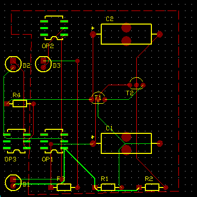
Hatched Copper Pour Area
1. Select a project from EDWinXP-Main → Open Project
2. Click on PCB Layout→ Edit PCB Layout . A window will appear.
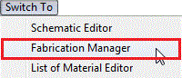
3. Click on Switch To→ Fabrication Manager
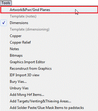
4. In the new window that appears,Click on Tools→Artwork&Pwr/Gnd Planes
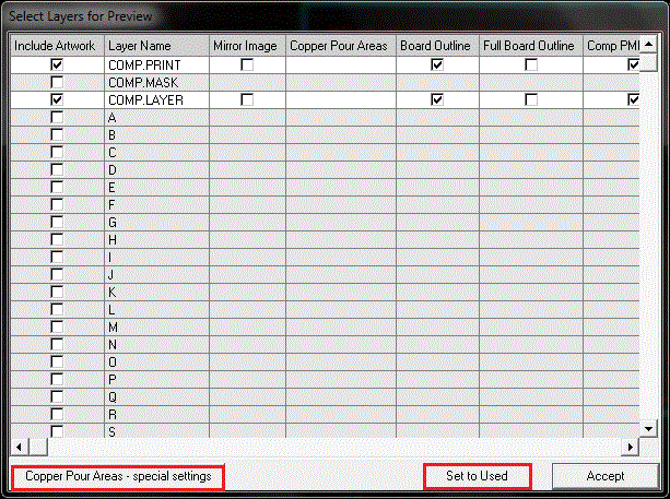
5. In the window that appears,Click on Set to Used, then on Copper Pour Areas-special settings
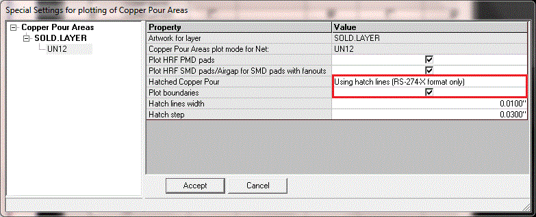
6. In the window that appears,Select Hatched Copper Pour as Using hatch lines(RS-274-X format only) and check the Plot boundaries,Click on Accept→Accept
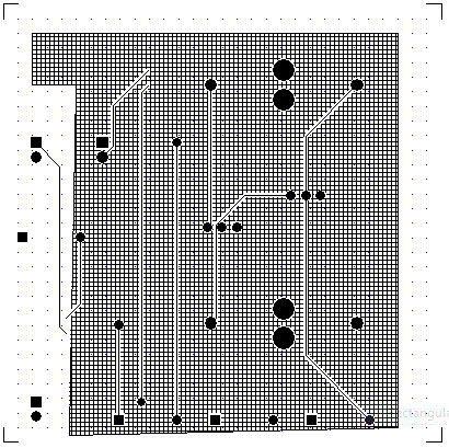
Output window is shown below
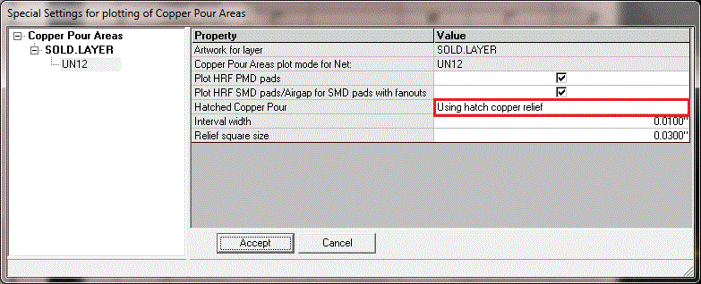
7. Select Hatched Copper Pour as Using hatch copper relief,Click on Accept→Accept
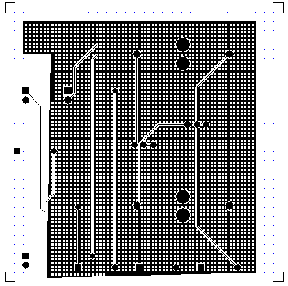
Output window is shown below
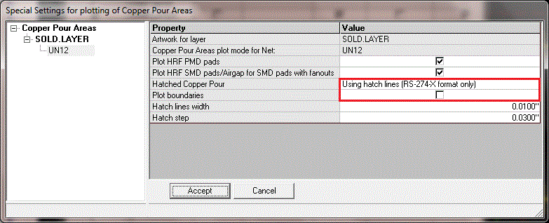
8. Select Hatched Copper Pour as Using hatch lines(RS-274-X format only) and Uncheck the Plot boundaries,Click on Accept→Accept
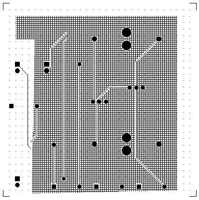
Output window is shown below
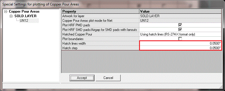
9. Change Hatch lines width & Hatch step,Click on Accept→Accept
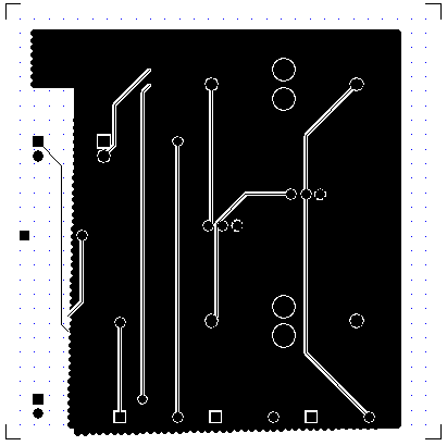
Output window is shown below

2. Click on PCB Layout→ Edit PCB Layout . A window will appear.
3. Click on Switch To→ Fabrication Manager
4. In the new window that appears,Click on Tools→Artwork&Pwr/Gnd Planes
5. In the window that appears,Click on Set to Used, then on Copper Pour Areas-special settings
6. In the window that appears,Select Hatched Copper Pour as Using hatch lines(RS-274-X format only) and check the Plot boundaries,Click on Accept→Accept
Output window is shown below
7. Select Hatched Copper Pour as Using hatch copper relief,Click on Accept→Accept
Output window is shown below
8. Select Hatched Copper Pour as Using hatch lines(RS-274-X format only) and Uncheck the Plot boundaries,Click on Accept→Accept
Output window is shown below
9. Change Hatch lines width & Hatch step,Click on Accept→Accept
Output window is shown below