PCB Wizard

Introduction
PCB wizard is a new tool which helps EDWinXP users to create the board automatically. It facilitates automatic placing and routing of components in a few steps. Proper settings have to be done on each step for the perfect completion of the board.
Procedure:
The components of the schematic are packed either by manual or auto packaging. Then invoke the Layout Editor. The packaged components will be stacked at the board datum.
Select Tools -> PCB Wizard. A window will be popped up as shown below. (Fig 1)
The required parameters are entered in the fields.
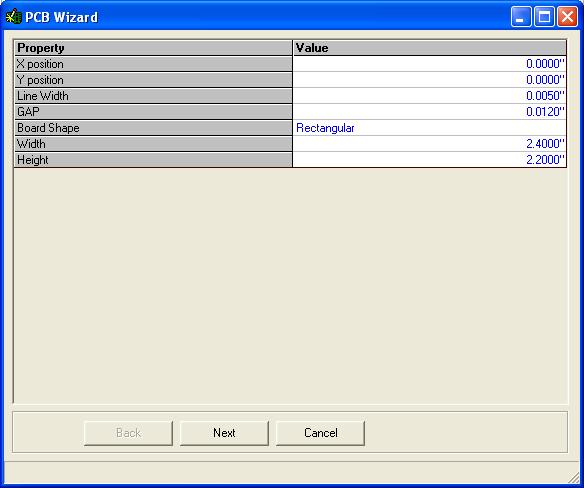
Fig 1
Click Next.
The parameters for autoplacing are set according to the requirement in the next window. (Fig2). The circuit design rules can be set in the section for Design rules.
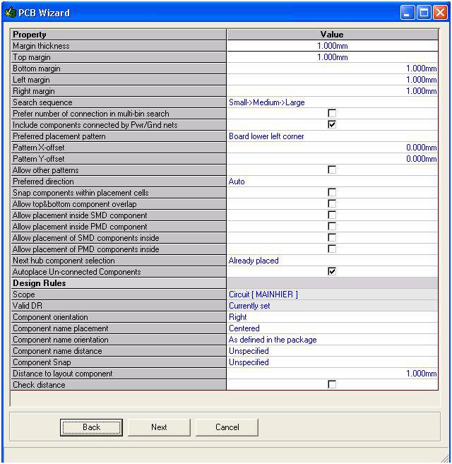
Fig 2
Click Next.
In the next window, (Fig 3) if no separate routing parameters are provided, the PCB wizard will take the default values from the circuit design rules to place and route the board.

Fig 3
You can also browse and input the routing parameters if necessary. The parameters can also be changed/ edited from the Routing Parameter Settings window. (Fig 4)

Fig 4
If any routing parameter is changed and when the Accept button is clicked, it will prompt to override rules specified in Circuit Design Rules. (Fig 5)

Fig 5
Click on Yes

Fig 6
After the completion of the automatic placing and routing, if any unrouted connections are present, it will list in the Display List of Unrouted Connections field. Click on Finish to exit the PCB wizard. (Fig 6)