Biased Double Limiter
Aim
To design and simulate a Biased Double Limiter circuit.
Components
|
Name
|
EDWin Components Used |
Description |
Number of components required |
| RES |
RC05 |
Resistor |
1 |
| DIODE |
1N4007 |
Diode |
2 |
| VGEN |
VGEN |
Ac voltage source |
1 |
| VDC |
VDC |
DC voltage source |
2 |
| GND |
SPL0 |
Ground |
1 |

Theory
Limiter is a
wave shaping circuit used to limit ac voltage to predetermined level. Limiters can transform a
sine wave into rectangular wave, can limit either the –ve or +ve alternation or
both alternations of an ac voltage. The diode limiters are also known as clippers. Limiters
may be classified as Series limiter and Parallel limiter depending on whether the output is taken
from the load resistor in series with the diode or in parallel with it.
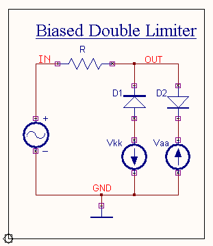
Circuit Operation: As shown
in the above circuit diagram two biased diode limiters are connected in
parallel such that the circuit acts as a partial limiter of both the +ve and –ve alternations. During the +ve half cycle of
the input voltage D1 remains in the reverse biased state. D2 also remains
in the reverse biased state until the input voltage
reaches the bias voltage Vaa Thus the output voltage follows the
input until D2 is forward biased. Thereafter the output remains constant at Vaa.
During the –ve half cycle of
the input voltage D2 remains in the reverse biased state. D1 also remains
in the reverse biased state until the input voltage
becomes more -ve than the bias voltage Vkk. Thus the output voltage follows
the input until D1 is forward biased. Thereafter the output
remains constant at Vkk.
The output waveform will be a sine wave clipped at >aa in the + ve half cycle and at Vkk in
the – ve half in
the – ve half cycle.
Thus the diode limiter modifies the input waveform by
limiting part of that waveform thereby changing the shape of the input waveform
whose extremities has been squared off.
Procedure
EDWinXP-> Schematic Editor:
The circuit diagram is drawn by
loading components from the library. Wiring and proper
net assignment has been made. The
values are assigned for relevant components.
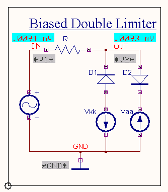
EDWinXP-> Mixed Mode Simulator: The circuit is preprocessed. The test points and waveform
markers are placed at input and output. The Transient Analysis parameters have been set.
The Transient Analysis is executed and output waveform is observed in the
Waveform Viewer.

Result
The output waveform may be observed in the waveform viewer.
