Monostable Multivibrator using 555
Aim
To simulate a monostable multivibrator using IC 555.
Components
Name |
EDWin Components Used |
Description |
Number of components required |
| RES | RC05 | Resistor | 1 |
| CAP | CAP | Capacitor | 2 |
| 555 | LM555 | Timer | 1 |
| VDC | VDC | Dc voltage source | 1 |
| GND | SPL0 | Ground | 3 |
| VGEN | VGEN | Pulse Generator | 1 |
Theory
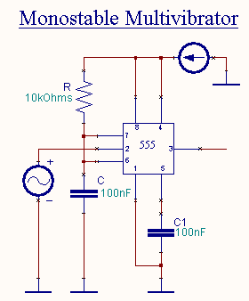
The 555 timer configured for monostable operation is shown in the figure.

Monostable multivibrator often called a one shot multivibrator is a pulse generating circuit in which the duration of this pulse is determined by the RC network connected externally to the 555 timer. In a stable or standby state, the output of the circuit is approximately zero or a logic-low level. When external trigger pulse is applied output is forced to go high (» VCC). The time for which output remains high is determined by the external RC network connected to the timer. At the end of the timing interval, the output automatically reverts back to its logic-low stable state. The output stays low until trigger pulse is again applied. Then the cycle repeats. The monostable circuit has only one stable state (output low) hence the name monostable.
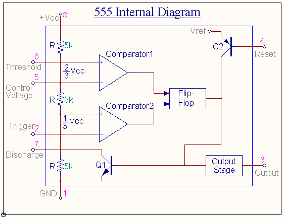
The internal diagram for a 555 timer is shown in the figure.

Pin1: Ground. All voltages are measured with respect to this terminal.
Pin2: Trigger. The output of the timer depends on the amplitude of the external trigger pulse applied to this pin.
The output is low if the voltage at this pin is greater than 2/3 VCC. When a negative going pulse of amplitude greater than 1/3 VCC is applied to this pin, comparator 2 output goes low, which inturn switches the output of thetimer high. The output remains high as long as the trigger terminal is held at a low voltage.
Pin3: Output. There are two ways by which a load can be connected to the output terminal: either between pin 3 and ground or between pin3 and supply voltage +VCC. When the output is low the load current flows through the load connected between pin3 and +VCC into the output terminal and is called sink current. The current through the grounded load is zero when the output is low. For this reason the load connected between pin 3 and +VCC is called the normally on load and that connected between pin 3 and ground is called normally off-load. On the other hand, when the output is high the current through the load connected between pin 3 and +VCC is zero.
The output terminal supplies current to the normally off load. This current is called source current.
The maximum value of sink or source current is 200mA.
Pin4: Reset. The 555 timer can be reset (disabled) by applying a negative pulse to this pin. When the reset function is not in use, the reset terminal should be connected to +VCC to avoid any possibility of false triggering.
Pin5: Control Voltage. An external voltage applied to this terminal changes the threshold as well as trigger voltage. Thus by imposing a voltage on this pin or by connecting a pot between this pin and ground, the pulse width of the output waveform can be varied. When not used, the control pin should be bypassed to ground with a 0.01µF Capacitor to prevent any noise problems.
Pin6: Threshold. This is the non-inverting input of comparator 1, which monitors the voltage across the external capacitor. When the voltage at this pin is greater than or equal to the threshold voltage 2/3 VCC, the output of comparator 1 goes high, which inturn switches the output of the timer low.
Pin7: Discharge. This pin is connected internally to the collector of transistor Q1. When the output is high Q1 is OFF and acts as an open circuit to external capacitor C connected across it. On the other hand, when the output is low, Q1 is saturated and acts as a short circuit, shorting out the external capacitor C to ground.
Pin8: +VCC. The supply voltage of +5V to + 18V is applied to this pin with respect to ground.
Operation
Initially when the circuit is in the stable state i.e , when the output is low, transistor Q1 is ON and the capacitor C is shorted out to ground. Upon the application of a negative trigger pulse to pin 2, transistor Q1 is turned OFF, which releases the short circuit across the external capacitor C and drives the output high. The capacitor C now starts charging up towards VCC through R. When the voltage across the capacitor equals 2/3 VCC, comparator 1’s output switches from low to high, which inturn drives the output to its low state via the output of the flip-flop. At the same time the output of the flip-flop turns transistor Q1 ON and hence the capacitor C rapidly discharges through the transistor. The output of the monostable remains low until a trigger pulse is again applied. Then the cycle repeats.The pulse width of the trigger input must be smaller than the expected pulse width of the output waveform. Also the trigger pulse must be a negative going input signal with amplitude larger than 1/3 VCC.
The time during which the output remains high is given by
t = 1.1RC seconds, where R is in Ohms and C is in Farads.
Once triggered, the circuit’s output will remain in the high state until the set time, t elapses. The output will not change its state even if an input trigger is applied again during this time interval t. The circuit can be reset during the timing cycle by applying negative pulse to the reset terminal.
The output will remain in the low state until a trigger is again applied.
Procedure
EDWinXP -> Schematic Editor: The circuit diagram is drawn by loading components from the library. Wiring and proper net assignment has been made. Values are assigned for relevant components.

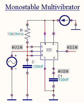
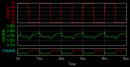
EDWinXP -> Mixed Mode Simulator: The circuit is preprocessed. The waveform marker is placed at the output of the circuit. GND net is set as the reference net. The Transient Analysis parameters are also set and the Transient Analysis is executed. The output waveform is observed in the Waveform Viewer.
Result
The output waveform may be observed in the waveform viewer.
