Zero Crossing Detector
Aim
To design and simulate a Zero Crossing Detector circuit.
Components
Name |
EDWin Components Used |
Description |
Number of components required |
| TRANSFORMER | SMB_TRANSFORMER | Transformer | 1 |
| RES | RC05 | Resistor | 3 |
| DIODE | 1N4007 | Diode | 5 |
| VGEN | VGEN | Ac voltage source | 1 |
| GND | SPL0 | Ground | 1 |
| NPN | BC107 | Transistor | 1 |
| CAP | CAP | Capacitor | 1 |
Theory
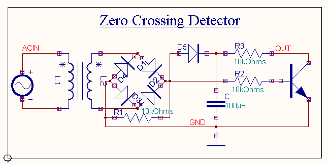
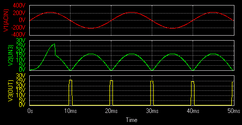
As the name indicates the zero crossing detector is a device for detecting the point where the voltage crosses zero in either direction. As shown in the above circuit diagram the first section is a bridge rectifier, which provides full wave rectified output. This is applied to the base of the transistor through a base resistor, R2. The capacitor charges to maximum of the bridge rectified output through the diode,D5. This charge is available to the transistor as VCC. The capacitance value is kept large in order to minimize ripple and get perfect dc. The transistor remains OFF until the Cut-in voltage VBE is reached. During the OFF period of the transistor the output will be high and approximately equal to VCC. Once the transistor is ON and IB increases according to the input wave, the transistor moves slowly towards saturation where the output reduces to the saturation voltage of the transistor which is nearly equal to zero.
Initially VBE = Cut-in voltage of diode, the
capacitor will charge through the diode![]() Vm where Vm
is
the maximum amplitude of the rectified wave. Now
the diode is reverse biased and hence does not provide a discharging path for the
capacitor, which in turn has two effects.
Vm where Vm
is
the maximum amplitude of the rectified wave. Now
the diode is reverse biased and hence does not provide a discharging path for the
capacitor, which in turn has two effects.
- Variation in VCC.
- It will provide base current to the transistor in the region where both diode and transistor are OFF.
Thus an output square wave is produced whenever the input voltage crosses zero thereby acting as a zero crossing detector.
Procedure
EDWinXP -> Schematic Editor: The circuit diagram is drawn by loading components from the library. Wiring and proper net assignment has been made. The values are assigned for relevant components.
EDWinXP -> Mixed Mode Simulator: The circuit is preprocessed. The waveform markers are placed at transformer primary, bridge output and detector output. The Transient Analysis parameters have been set. The Transient Analysis is executed and output observed in the Waveform Viewer.
Result
The output waveform may be observed in the waveform viewer.