V.I. Characteristics of Zener Diode
Aim
To plot the VI characteristics of a Zener diode.
Components
Name |
EDWin Components Used |
Description |
Number of components required |
| RES | RC05 | Resistor | 1 |
| ZENER | 1N3828 | Zener Diode | 1 |
| VGEN | VGEN | Ac voltage source | 1 |
Theory
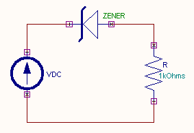
The circuit diagram to plot the VI characteristics of a zener diode is shown. Zener doide is a special diode with increased amounts of doping. This is to compensate for the damage that occurs in the case of a pn junction diode when the reverse bias exceeds the breakdown voltage and thereby current increases at a rapid rate.
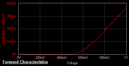
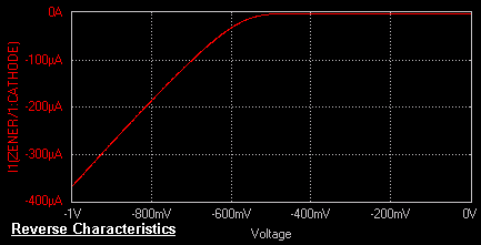
Applying a positive potential to the anode and a negative potential to the cathode of the zener diode establishes a forward bias condition. The forward characteristic of the zener diode is same as that of a pn junction diode i.e. as the applied potential increases the current increases exponentially. Applying a negative potential to the anode and positive potential to the cathode reverse biases the zener diode. As the reverse bias increases the current increases rapidly in a direction opposite to that of the positive voltage region. Thus under reverse bias condition breakdown occurs. It occurs because there is a strong electric filed in the region of the junction that can disrupt the bonding forces within the atom and generate carriers. The breakdown voltage depends upon the amount of doping. For a heavily doped diode depletion layer will be thin and breakdown occurs at low reverse voltage and the breakdown voltage is sharp. Whereas a lightly doped diode has a higher breakdown voltage.
This explains the zener diode characteristics in the reverse bias region.
The maximum reverse bias potential that can be applied before entering the zener region is called the Peak Inverse Voltage referred to as PIV rating or the Peak Reverse Voltage Rating (PRV rating).
Procedure
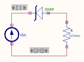
EDWinXP-> Schematic Editor: The circuit diagram is drawn by loading components from the library. Wiring and proper net assignment has been made. The resistor R is assigned a proper value. For obtaining reverse bias the anode and cathode of zener diode is swapped.
EDWinXP -> Mixed Mode Simulator: The circuit is preprocessed. The VI characteristics may be obtained by performing DC Sweep Analysis. The current waveform marker is placed at the cathode of the diode. The sweep parameter (voltage) for input source is set in the Analysis window. The applied voltage is swept from an initial value of 0 to final value of 1V in steps of 1mV. To get VI characteristics, the currents corresponding to varying input voltages are noted. The VI graph is observed in the Waveform Viewer.
Result
The output waveform may be observed in the waveform viewer.