Via Stiching
The stitching via electrically connects the reference planes. It reduces the area of the signal current flow, noise and crosstalk on the PCB.
Creating Stitching Via :
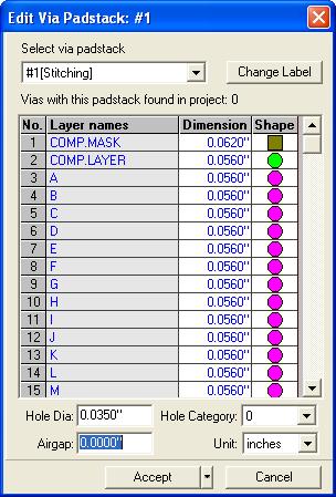
- Evoke Default Via Padstack Editor from System /Project Explorer. Edit via Padstack window appears as shown in figure below.
- Select via padstack from the Select via padstack drop down.
- Assign the airgap size as ‘zero’.
- Click Accept to use the values for the current project or click Save & Exit (press the arrow next to Accept to view this button) if the values are to be preserved for future projects.
Using Stitching via’s in the project :
- Select stitching via from the via pad drop down menu in sizes too tool bar.
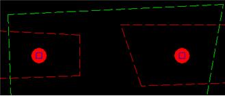
- SelectCreate Via option tool from Edit Via function tools of Tools Connections and click on the graphics area to get the selected via pad tagged to the cursor. Move the cursor to the required location and click to place it.Keep the stitching via in such a way that it connects the copper planes.
- The stitching via electrically connects the copper planes. Click on 3D trace viewer to view the 3D Trace view.
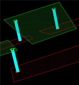
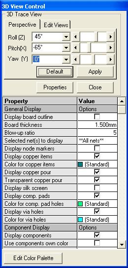
Tip : You can set properties in 3D trace viewer as shown in figure below to get the above view
Note:To check connectivity, execute connectivity check, Copper pour connectivity check, Shortcuts to copper pour check etc.
If you require an intermediate copper plane between the specified layers, the stitching via can be created by any of the following 3 steps.
- 1. A pad can be created as a part with airgap zero and place the part by loading
it from the library.
2. Place copper relieve item on the stitching via from the fabrication manager so that the plane in the intermediate layer gets isolated so that no connections are created.