Sweep Generator
Aim
To simulate a transistor sweep generator circuit.
Components
|
Name |
EDWin Components Used |
Description |
Number of components required |
| TRANSISTOR | BC107A | NPN Transistor | 1 |
| RES | RC05 | Resistor | 2 |
| CAPACITOR | CAP | Capacitor | 1 |
| VGEN | VGEN | Voltage Generator | 1 |
| VDC | VDC | Voltage source | 1 |
| GND | SPL0 | Ground | 1 |
Theory
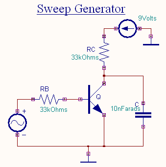
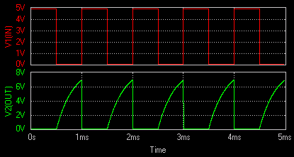
The circuit diagram of a transistor sweep generator is shown in the figure. The performance of the circuit can be explained as follows. During the positive half cycle of the input signal the base-emitter junction of the transistor becomes forward biased. The transistor conducts and is driven into saturation. Then the output voltage will be low. During the negative half cycle the base-emitter junction becomes reverse biased and the transistor is driven into cut-off. During this interval the collector of the transistor will be at a voltage slightly less than VCC. The capacitor now charges towards this high voltage. During the next positive half cycle the transistor turns ON and provides the discharge path for the capacitor. The capacitor discharges during the short time interval. Thus during the positive half cycle the output of the circuit will be low and during the next half cycle we obtain the sweep wave in the output. Hence the name sweep generator for the circuit.
Procedure
EDWinXP -> Schematic Editor: The circuit diagram is drawn by loading components from the library. Wiring and proper net assignment has been made. Values are assigned for relevant components
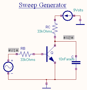
EDWinXP -> Mixed Mode Simulator: The circuit is preprocessed. The waveform markers are placed at the input and output of the circuit. GND net is set as the reference net. The Transient Analysis parameters are also set and the Transient Analysis is executed. The output waveform is observed in the Waveform Viewer.
Result
The output waveform is observed in the waveform viewer.