Schmitt Trigger
Aim
To design and simulate a Schmitt Trigger circuit.
Components
Name |
EDWin Components Used |
Description |
Number of components required |
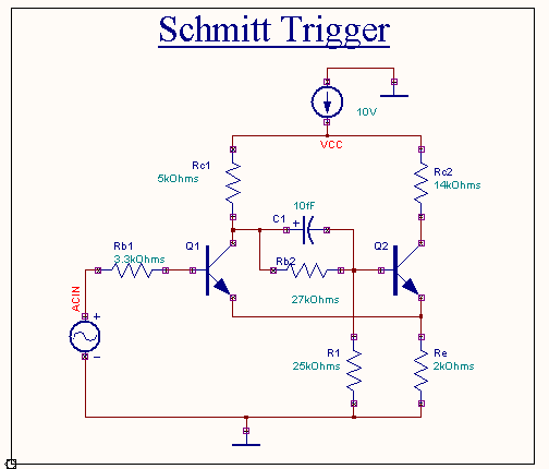
| BC107 | BC107A | Transistor | 2 |
| RES | RC05 | Resistor | 6 |
| CAP | CASE-A600 | Capacitor | 1 |
| VGEN | VGEN | Ac voltage source | 1 |
| VDC | VDC | Dc voltage source | 1 |
| GND | SPL0 | Ground | 1 |
Theory
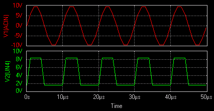
Schmitt Trigger is an emitter coupled binary trigger circuit. It is termed a binary trigger circuit since two stable states occur- the transistor Q1 may be ON and Q2 OFF or vice versa. In the absence of an input to transistor Q1 the voltage divider network Rb2 and R1 along with Rc1 maintains the base of Q2 at a slightly positive potential relative to the emitter and thereby Q2 operates in the saturation region. Owing to the current flow in Q2, the voltage developed across the common emitter resistor, Re maintains Q1 at cut-off. Since the base of Q1 is at ground potential, it is negative relative to the emitter. Thus the stable state in the absence of a signal is Q2 ON and Q1 OFF and the output voltage is in the low state. The switching action may be started by raising or lowering the bias on Q1.When an input sine wave is applied, as soon as the input voltage attains a value equal to the sum of the voltages across Rb1 and Re, Q1 turns ON since its base becomes more positive relative to the emitter. Q1 is driven to conduction in the saturation region. The collector voltage of Q1 drops, which inturn is coupled by the network Rb2-R1 to the base of Q2. This eliminates the forward bias on Q2 and hence it is driven to cut-off. This state persists as long as the input voltage is greater than the sum of the voltages across Rb1 and Re. When Q2 is driven to cut-off, output voltage switches to the difference between Vcc and the voltage across Rc2.
When the input voltage drops below the sum of the voltages across Rb1 and Re Q1 turns OFF and by regenerative action Q2 again turns ON. The output voltage falls back to the sum of the voltages across Re and the saturation voltage of Q2. Thus a square wave is produced. The turn ON voltage is usually called the upper trigger point or UTP and the tun OFF voltage is called lower trigger point or LTP. UTP is always greater than LTP since the voltage required to turn ON a device is more than that required to turn it OFF.
Design
Design Specifications
![]()
![]()
![]()
![]()
Manufacturers specifications
![]()
![]()
Initially Q1 is OFF and Q2 is ON
![]()
![]()
![]()
![]()
From equations (1) and (2)
![]()
![]()
![]()
Applying KVL to the output side of the circuit,
![]()
![]()
![]()
![]()
![]()
![]()
![]()
![]()
According to Ohm’s law
![]()
i.e. ![]()
![]()
When Q1 is ON and Q2 is OFF
![]()
![]()
![]()
![]()
![]()
![]()
Applying KVL
![]()
![]()
![]()
![]()
![]()
From equation (9)
![]()
The condition for stability is
![]()
We take
![]()
![]()
C1 should be properly selected in order to get perfect output.
Select C1 as 100pF.
Procedure
EDWinXP -> Schematic Editor: The circuit diagram is drawn by loading components from the library. Wiring and proper net assignment has been made. The values are assigned for relevant components.
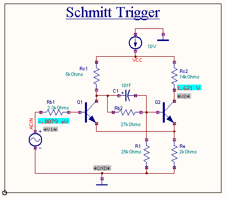
EDWinXP> Mixed Mode Simulator: The circuit is preprocessed. The desired test points and waveform markers are placed. The Transient Analysis parameters have been set. The Transient Analysis is executed and output observed in Waveform Viewer.
Result
The output waveform may be observed in the waveform viewer.