RC COUPLED AMPLIFIER
Aim
To simulate the RC coupled amplifier
Components required
Transistor – BC107A (1), Resistor – RC05 (6), Capacitor – CK05 (2), CASE-AA100 (1), AC Voltage Source – VGEN (1), DC Voltage Source – VDC (1), Ground – SPL0 (2)
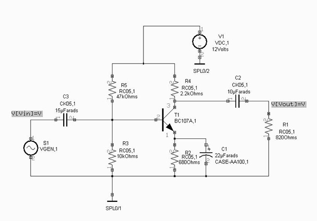
Circuit Diagram
Procedure
1) Loading/Placing of components
Components can be loaded in the schematic page by selecting Tools--> Components--> Add components to the circuit (first function tool) -->Add components by name (third option tool) Enter the part name in the input box & click Accept
Components are created in unlimited repeat mode, use ESC key to end the component repeat. The components can be placed in the grids with 100 mils (.1”) and snap of 50 mils (.05”) in the required position by relocation. For relocating a placed component, Tools--> Components -->Relocate component, click on the component which have to be relocated and place it on the required position. Press Redraw button for refreshing the page if necessary
# It is possible to use the customized keyboard keys for easy placement of components Say press R for resistor, C for capacitor, Q for transistor, V for voltage generator, G for ground etc
2) Routing Connections
The connection between components can be made by Tools --> Connections --> Connect components (First Function tool) {Connect the wires from pin to pin according to the circuit diagram.} .Press F4 or keyboard END key for ending the connection and Esc button for cancel the connection.
Note: The logical connections are made only when the node connections are established
# Do not rename the ground net SPL0 to other names like Ground, GND etc. # Do not rename SPL1 to other names like Supply, VCC etc. # Select Tools-> Connections--> Connection properties--> Click on any connection and name it as required. Assign net names for connections wherever necessary.
3) Simulation
Draw the circuit diagram after loading components from library. Assign net names for connections wherever necessary. Preprocess the circuit by invoking Simulation --> Preprocess. Place waveform markers on input and output nodes. For placing waveform markers, select Tools -->Instruments --> set wave form Contents --> Voltage waveform --> Click on the required net and place the waveform marker.
To proceed with the simulation, the steps are as follows
Select Tools --> Components --> Component properties -->Change simulation parameters-->Click on the required component and change its values.
The values to be provided to the components are
Transistor : BC107A (Click on the Set up Model of the Model Type. Click on Accept to get the default values assigned)
Resistors : R1 = 47k, R2 = 10k, RC = 2.2k, RE = 680 Ohm, RL = 1k
Capacitors : CC1 = 1µF, CC2 = 1µF, CE = 10µF
VDC/1 (+Vcc) : 10V
VGEN : Select the source function as SIN and set its Properties as follows
VA (Amplitude) : 10mV
FREQ (Frequency) : 10kHz
Analysis
Select Simulation -->Analysis
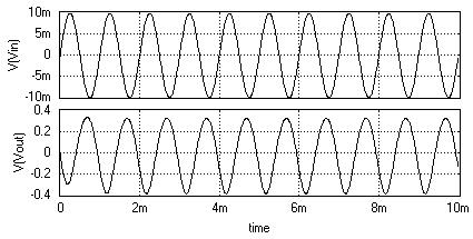
Transient Analysis
Transient analysis is used to view input and output with respect to time.
1. Select Simulation --> Analysis
2. Select Transient Analysis from the tree view
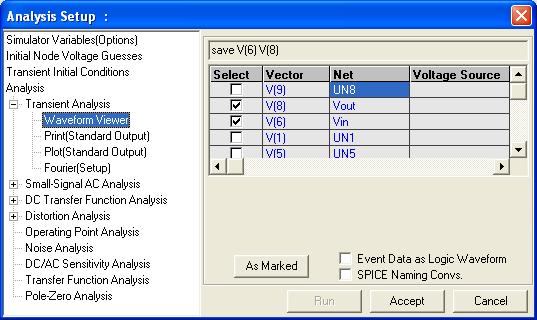
3. Expand Transient Analysis and select Waveform Viewer
4. Click on the As Marked button and then on Accept
5. Click on the Transient Analysis
6. Enter the values as
Step : 10µ
Final time : 10m
Start time : 0
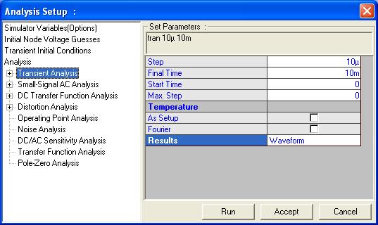
7. Click Accept button after entering the values.
8. Click Run button to start simulation.
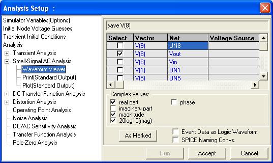
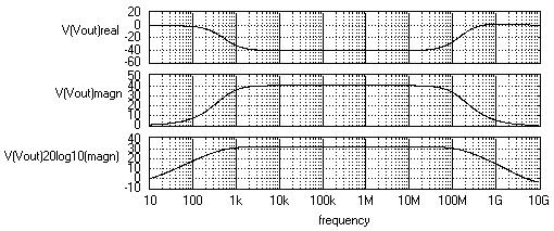
Small Signal AC Analysis
This analysis is used to obtain the small signal AC behaviour of the circuit.
1. Select Simulation --> Analysis.
2. Select Small Signal AC Analysis from the tree view.
3. Expand Transient Analysis and select Waveform Viewer.
4. Select the required Complex values and then click on Accept.
5. Enter the values for the Small-Signal AC Analysis as
Total points : 100
Start frequency : 10 Hz
End frequency : 10G
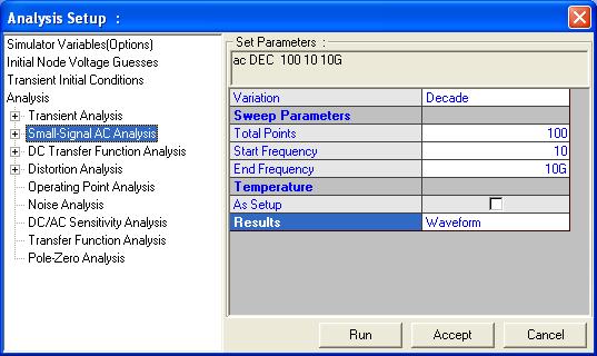
6. Select Waveform for displaying the output.
7. Click Accept button after entering the values to automatically switch to Analysis.
8. Click Run button to start simulation
Simulation using Circuit (CIR) files
Procedure
Open CIR file Editor from Simulation-->Circuit File Editor
Type the circuit description in the editor and save the file with cir file extension.
Click Simulate to run the simulation.
Example
RC INTEGRATOR
VIN 1 0 PULSE (-10 10 0 0 0 .5M 1M)
R1 1 2 1K
C1 2 0 0.1U
.TRAN 10U 5M
.SAVE V(1) V(2)
.END
PCB Layout
For packing the components, Schematic Editor -->Tools --> Components --> Pack/ Unpack Component --> Auto Packaging. Click on Execute. The components will be front annotated to the Layout Editor
PCB Layout is invoked from Project Explorer in the following ways.
Right click PCB Layout and select Edit PCB Layout from the list. Or Select Edit PCB Layout from the task list or from the task toolbar.
Define board outline
1. Select Tools --> Board Outline
2. Select Define Outline (function tool) --> Create Board (option tool). This tool enables free hand drawing, using which a board of desired shape can be drawn on the workspace.
3. To select a pre-defined board format, select the option tool Textual Mode. The Properties Board Outline (Create) dialog pops up.
4. Enter the desired values and click Accept button.
Relocating the components
The components placed on the schematic, which contain both symbol and package, are front annotated to the layout after packaging. These components are positioned at board datum (0,0) automatically and may be relocated either manually or automatically
Note: Only parts that contain both symbol and package will be automatically back annotated to the schematic
1. Before we start loading Parts on to the page, turn ON Grid by enabling grid from the dropdown, in Standard Toolbar. The value for grid may be selected from the drop down list as .1000”.
2. Similarly, set Snap value to .0500” for better placement of the components.
3. Select Tools--> Components--> Relocate Component (function tool) to relocate the components.
4. Enable Ratsnest (F7 key) option tool of Relocate Component function tool to view ratsnest while relocating the components to ensure that components having a large number of interconnections are positioned close to each other. Pressing shift key while relocating/ stretching an item allows the item to move/ stretch smoothly.
Routing the Components
Connections between components may be established by using Traces and Copper Pour areas.
1. Select Tools -->Connections --> Route (Function tool) to enable a set of Routing tools on right clicking the workspace.
2. Adjust zoom precision to view the pins properly.
3. Turn on Preference/ Guidelines (Next unconnected node) before routing because this option guides you to take the easiest path to route.
4. Select True Size and Pad frames from View/ Layout, enabling you to select proper trace size. This also prevents you from creating errors such as traces crossing over pad, traces very close together etc.
5. First route power and ground signals (Net SPL0 and +5V). In Project Explorer, select Project / Project Design Rules and set the routing width to 0.030” for Pwr/Gnd lines and 0.013” for Signal lines.
6. To start routing traces, first select the power points
7. Select layer for routing from Layers in the main menu. 28 layers are available for routing. By default COMP LAYER is selected. Click on pin to route on SOLD LAYER.
Tips: While routing, enable the tool Snap Trace by 45 degree to change routing directions in steps of 45 deg only.
8. Move cursor with 45° angle through a short distance and click at the nearest point.
9. Terminate routing of the trace by pressing END or F4 key on your keyboard. Or click on the tool End Connections.
Arizona Autorouter
Arizona auto router is an integrated module of the EDWinXP. It uses its own temporary project and simplified graphics. The Arizona auto router allows routing the traces of a PCB Layout automatically
Auto routing using Arizona Auto router
1. Select Auto --> Auto Router -->Arizona.
2. Select File -->Load board to route from project.
3. Select Parameters Setup (function tool)--> Routing Parameter Settings (option tool).
4. Check Solder Layer in the Routing Parameters Settings window
5. Select Auto routing Routines (function tool) -->Start Auto Router.
6. Select Auto routing Routines --> Miter.
7. Close Arizona Auto router window, Click Update project and Exit to save the project.
Testing the Board
While designing a PCB, it is quite obvious that a number of errors may occur. These errors may be in the form of overlapping pads, unconnected Nodes, traces crossing another trace, etc. Such errors must be taken care of before printing the PCB. To find out such errors, certain checks on the board are done. Connectivity and DRC check are the two checks.
Connectivity Test
Connectivity test may be used to check whether there is any electrical discontinuity (unconnected nodes or deleted trace segments) in a single net. By setting certain parameters, the test can be performed either on individual nets or all the selected nets.
1. Select Tools --> Connections--> Connection Property -->Test Connectivity
2. Click on the board or on a net. The Connectivity Test dialog pops up.
3. Select the required nets using the move keys and click the connectivity test tab.
4. Select Connectivity test tab, set anyone of the three options:
Stop at first fail: Test stops at the first occurrence of error.
Test all selected Nets: Checks whether all Nodes of the selected Nets are connected.
Test single Net: Checks connectivity of the Nodes of the selected Net.
5. Click the Test button to display the results.
6. Perform this test until “Tested Nets – Fully Connected” message is displayed in this window.
Design Rule Check (DRC)
This utility is used to create an error free board to enhance the efficiency of your board. It automatically smoothes, miters, and checks for both aesthetic and manufacturing problems that might have been created in the process of manual or automatic routing. This test helps us to check the clearance between pad to pad, pad to trace and trace to trace.
1. Select Autocheck from Auto Menu. The Clearance Check dialog pops up.
2. Select the layers and enter the clearance value in the window.
3. To select all the layers used in the project click the Set To Used button
4. Click Execute.
3D Board Viewer
3D Board Viewer gives idea on how the components are located, whether there is risk of friction between components due to their height and shape, the side on which components are placed, etc.
Select Layout Editor --> Tools --> 3D Board Viewer to view the 3D board
3D View Control box appears, in this we can select options to view the board in any direction.
FABRICATION MANAGER
Introduction
Fabrication is the last stage of the electronic design process. The PCB information is converted into ASCII output files – GERBER (.gbr), NC Drill (.ncd), PCB Assembly Outputs Generic (.pck), IPC-D-355(.355), Bare Board Testing Generic (.bbt) and IPC-D-356A(.356) which are input to machines to finally create the hardware.
1. Invoke PCB Layout in the Project Explorer.
2. Select Fabrication Manager from the tasklist or Select from the task toolbar. The Fabrication Manager window opens with a default board size and gets aligned with the Project Explorer to fit the screen.
3. Invoke Fabrication Data Manager choose Setup from Fabrication.
4. Choose Gerber Artworks in the left pane of Fabrication Data Manager .
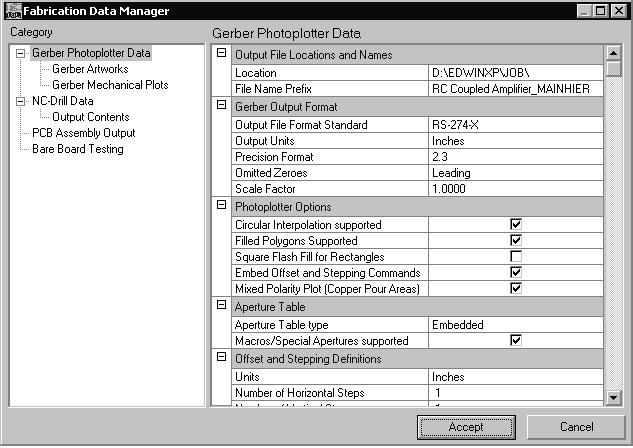
Gerber Output
GERBER is the standard format used as input to photoplotters that generate the design data on films. These films are used as masters for manufacturing the PCB, the physical realization of the schematic data. GERBER format is a vector format for defining various elements of the layout. This format represents all traces as draw and the pads that are part of the component footprint as flashes. The Photoplotter uses this command language
1. Select the layers for which we want the Gerber Artwork files.
2. Click on Execute.
3. ‘Gerber output window’ opens, Click on Execute.
4. This completes the generation of GERBER data.
Preview the GERBER Data
Fabrication Manager -->File--> Gerber/ Excellon/ DXF/HPGL Viewer-->“Select File for Import” window popups
Select .GBR file in the Files of Type and choose the required GBR file to open. A window named “Import Parameters” popups.
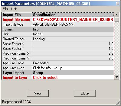
In the “Import to Layer” field, select the necessary layer to which the import of the specified layer has to be done. After the layer selection, click Close to exit the window.