Procedure for creating schematic diagram and simulating it
- Open EDWinXP from Start →Programs → EDWinXP - Main
- Click on File → New project for starting a new project
- Invoke the Schematic editor by double clicking the Project → Page (Mainpage)
Steps for simulation
- Placing the components
- Wiring the components
- Set the instance parameters for all components(component value)
- Feeding input signals
- Place wave form markers / probes for viewing the output
- Run simulation with suitable time step and time limit
EDSpice simulation
Select the EDSPICE simulator by
Preferences→EDSpice simulator
Steps i & ii should be completed before starting the simulation
Integrator
Aim
To simulate an integrator circuit.
Components Required
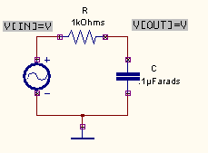
Resistor- RC05 (1), Capacitor- CC0805 (1), AC Voltage Source-VGEN (1), Ground- SPL0 (1)
Circuit Diagram
Procedure
1) Loading/Placing of components
- Components can be loaded in the schematic page by selecting the Tools→Components →Add components to the circuit (first function tool) →Add components by name (third option tool)
- Enter the part name in the input box & click Accept

- Components are created in unlimited repeat mode, use ESC key to end the component repeat. The components can be placed in the grids with 100 mils (.1”) and snap of 50 mils (.05”) in the required position by relocation.
- For relocating a placed component, Tools→Components →Relocate component, click on the component which have to be relocated and place it on the required position.
- Press Redraw button for refreshing the page if necessary
# It is possible to use the customized keyboard keys for easy placement of components Say press R for resistor, C for capacitor, Q for transistor, V for voltage generator, G for ground etc
2) Routing Connections
The connection between components can be made by Tools → Connections → Connect components (First Function tool) {Connect the wires from pin to pin according to the circuit diagram.} .Press
F4 or keyboard END key for ending the connection and
Esc button for cancel the connection.
Note: The logical connections are made only when the node connections are established.
# Do not rename the ground net SPL0 to other names like Ground, GND etc.
# Do not rename SPL1 to other names like Supply, VCC etc.
# Select Tools→Connections→Connection properties→Click on any connection and name it as required. Assign net names for connections wherever necessary. Here input is given as
IN and output is given as OUT
3) Simulation
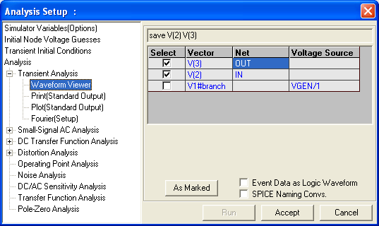
Preprocess the circuit by invoking Simulation → Preprocess. Place waveform markers on input and output nodes. For placing waveform markers, select Tools → Instruments → set wave form Contents → Voltage waveform → Click on net IN and place the waveform marker. Click on net OUT and place the waveform marker.
To proceed with the simulation, the steps are as follows
- Select Tools → Components → Component properties→ Change simulation parameters→ Select any component and change it values.
- The values to be provided to the components are
Resistors : 1k
Capacitors: 0.1µF
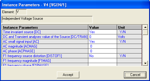
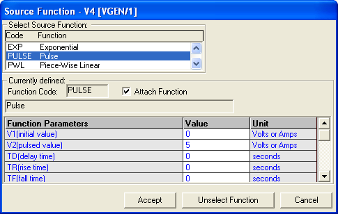
VGEN : Select the source function as PULSE and set its Properties as follows
V1 (Initial value) : 0V
V2 (Pulsed Value) : 5V
Pulse width : 0.5m
Period : 1m (All other values are zero)
Time invariant source [DC] – Yes
DC and Transient analyses values of the Source [DC/ TRAN]< – 0
AC small signal input [AC] – Yes
AC magnitude [ACMAG] – 0
AC phase [ACPHASE] - 0
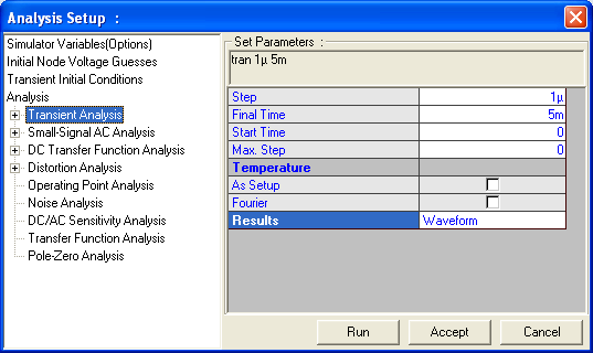
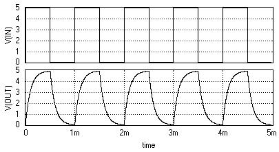
For setting up simulation time and analysis types, select Simulation menu, choose Analysis. In the window pops up, select Transient analysis from tree view.
Enter following values:
Step : 1µ
Final time : 5m
Results : Select Waveform from drop down menu.
Click on Accept.
Expand the Transient Analysis and select Waveform viewer, Select As Marked. Click on Accept.
Select Transient Analysis. Run Analysis by clicking on Run button.
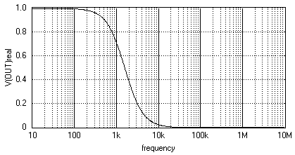
For performing the Small Signal AC Analysis, select Simulation → Analysis. Select Small Signal AC Analysis from the tree view. Enter the values as
Variation : Decade
Total Points : 100
Start Frequency : 10Hz
End Frequency : 10MHz
Results : Select Waveform for displaying the output.
Click Accept button after entering the values to automatically switch to Analysis. Click
Run button to start simulation
Result
Procedure
Open CIR file Editor from Simulation → Circuit File Editor
Type the circuit description in the editor and save the file with cir file extension. Click
Simulate to run the simulation
Example
RC INTEGRATOR
VIN 1 0 PULSE (-10 10 0 0 0 .5M 1M)
R1 1 2 1K
C1 2 0 0.1U
.TRAN 10U 5M
.SAVE V(1) V(2)
.END