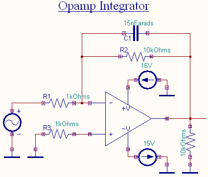
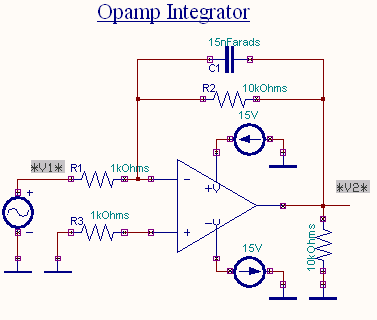
Opamp Integrator
Aim
To design and simulate an Integrator circuit using opamp.
Components
Name |
EDWin Components Used |
Description |
Number of components required |
| RES | RC05 | Resistor | 4 |
| CAP | CASE-A600 | Capacitor | 1 |
| OPAMP | 741A | Comparator | 1 |
| VGEN | VGEN | Ac voltage source | 1 |
| VDC | VDC | Dc voltage source | 2 |
| GND | SPL0 | Ground | 5 |
Theory
A circuit in which output voltage is directly proportional to the integral of the input is known as an integrator or the integration amplifier. Such a circuit is obtained by using operational amplifier in the inverting configuration with the feedback resistor RF replaced by a capacitor, CF.
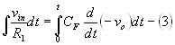
Applying KCL the expression for output voltage is obtained as follows.
![]()
Since IB is negligibly small
![]()
The current through the capacitor is related to voltage by the relation
![]()
Therefore,
![]()
However,
![]() because A is very
large. Therefore,
because A is very
large. Therefore,
![]()
![]()
The output voltage can be obtained by integrating both sides with respect to time,
Therefore
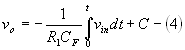
where C is the integration constant and is proportional to the value of the output voltage v0 at time t = 0 seconds. Equation 4 indicates that the output voltage is directly proportional to the negative integral of the input voltage and inversely proportional to the time constant R1CF.
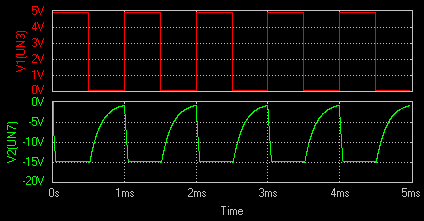
For example if the input is a sine wave, the output will be a cosine wave; or if the input is a square wave output is a triangular wave. When vin = 0, the integrator works as an open loop amplifier. This is because the capacitor CF acts as an open circuit to the input offset voltage vio. This input offset voltage and the part of the input current charging capacitor CF produce the error voltage at the output of the integrator. Therefore in a practical integrator, to reduce the error voltage at the output, a resistor RF is connected across the feedback capacitor CF. Thus RF limits the low frequency gain and hence minimizes the variations in the output voltage. The addition of the resistor also corrects the stability and low frequency roll-off problems. Considering the frequency response the limiting frequencies are defined as follows.
The frequency at which gain is 0dB is given by
![]()
The gain limiting frequency is given by
![]()
The circuit acts as an integrator in the frequency range fa to fb. the value of fa and in turn R1CF and RFCF values should be selected such that fa<fb. Thus the output is proportional to the time integral of the input.
Procedure
EDWinXP-> Schematic Editor: The circuit diagram is drawn by loading components from the library. Wiring and proper net assignment has been made. The values are assigned for relevant components.
EDWinXP-> Mixed Mode Simulator: The circuit is preprocessed. Waveform markers are placed at the input and output of the circuit. GND net is set as reference net. The Transient Analysis parameters have been set. The Transient Analysis is executed and output waveform is observed in the Waveform Viewer.
Result
The output waveform may be observed in the waveform viewer.