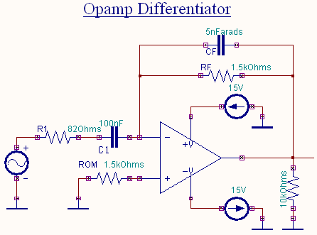
Opamp Differentiator
Aim
To design and simulate a Differentiator circuit using opamp.
Components
Name |
EDWin Components Used |
Description |
Number of components required |
| RES | RC05 | Resistor | 4 |
| CAP | CASE-A600 | Capacitor | 2 |
| OPAMP | 741A | Comparator | 1 |
| VGEN | VGEN | Ac voltage source | 1 |
| VDC | VDC | Dc voltage source | 2 |
| GND | SPL0 | Ground | 5 |
Theory
A circuit in which output waveform is the derivative of the input waveform is known as the differentiator or the differentiation amplifier. Such a circuit is obtained by using operational amplifier in the inverting configuration connecting a capacitor, C1 at the input. Applying KCL the expression for output voltage is obtained as follows.
![]()
Since ![]()
![]()
![]()
But ![]() because A is
very large. Therefore
because A is
very large. Therefore
![]()
![]()
Thus the output vo is equal to RFC1
times the negative instantaneous rate of change of the input voltage vin
with time. The gain of the circuit ![]() increases with increase in frequency at a rate of 20 dB/decade. This makes the circuit
unstable. Also the input impedance XC1 decreases with increase in frequency which makes
the circuit susceptible to high frequency noise. When amplified the noise
can completely override the differentiated output signal. The
frequency at which gain is zero dB is given by
increases with increase in frequency at a rate of 20 dB/decade. This makes the circuit
unstable. Also the input impedance XC1 decreases with increase in frequency which makes
the circuit susceptible to high frequency noise. When amplified the noise
can completely override the differentiated output signal. The
frequency at which gain is zero dB is given by
![]()
The stability and high frequency noise problems can be corrected by the addition of two components:- R1 and CF. The gain limiting frequency fb isgiven by
![]()
R1CF and RFCF
make the circuit more stable by preventing the increase in gain with frequency. The value
of fb and in turn R1C1
and RFCF values should be selected such that fa<fb<fc where ![]()
![]()
and fc is the unity gain bandwidth of the opamp. Thus the input signal will be differentiated properly if the time period of the input signal is larger than or equal to RFC1
i.e. ![]() .
.
Procedure
EDWinXP -> Schematic Editor: The circuit diagram is drawn by loading components from the library. Wiring and proper net assignment has been made. The values are assigned for relevant components.
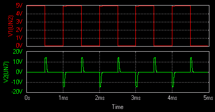
EDWinXP> Mixed Mode Simulator: The circuit is preprocessed. Waveform markers are placed at the input and output of the circuit. GND net is set as reference net. The Transient Analysis parameters have been set. The Transient Analysis is executed and output waveform is observed in the Waveform Viewer.
Result
The output waveform may be observed in the waveform viewer.