741 Non-Inverting Amplifiers
Aim
To design and simulate Summing and Averaging Amplifier circuits using 741.
Components
Name |
EDWin Components Used |
Description |
Number of components required |
| RES | RC05 | Resistor | 6 |
| COMPARATOR | LM358 | Comparator | 1 |
| VDC | VDC | Dc voltage source | 5 |
| GND | SPL0 | Ground | 7* |
Theory
An operational amplifier is a direct coupled high gain amplifier consisting of one or more differential amplifiers and usually followed by a level translator and an output stage which is usually a push-pull or push-pull complementary symmetry pair. An operational amplifier can be used to amplify ac as well as dc input signals and was originally designed for computing such mathematical functions as addition, subtraction, multiplication and integration.
An opamp can be configured in either the inverting or in the non-inverting mode. The circuit shown below is called a non-inverting amplifier, since the input voltage sources and resistors are connected to the non-inverting terminal of the op-amp. The circuit can be used either as a summing or an averaging amplifier through the selection of appropriate values of resistors, R1 and RF. The input resistance RiF of the non-inverting amplifier is very large and is given by
![]()
In order to verify the functions of the circuit, the expression for the output voltage can be obtained as follows. Applying the superposition theorem, the voltage V1 at the non-inverting terminal is
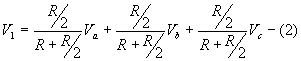
![]()
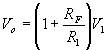
Hence the output voltage Vo is
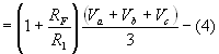
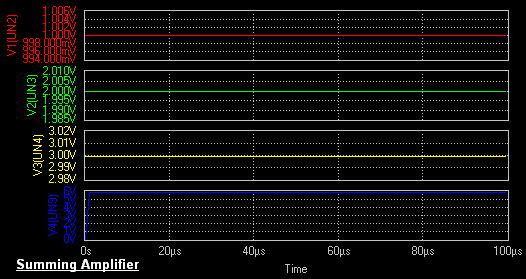
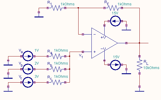
Summing Amplifier
The Summing Amplifier produced using 741 is the circuit that sums up
all the input voltages. As evident from equation 4 if the gain ![]() is equal to the number of inputs, the output voltage becomes equal to the sum of all input
voltages. That is, if
is equal to the number of inputs, the output voltage becomes equal to the sum of all input
voltages. That is, if ![]() , then
, then ![]() .
.
Hence the circuit is called a non-inverting summing amplifier.
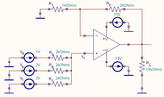
Averaging Amplifier
The output of the non-inverting amplifier as obtained from
equation 4 is equal to the average of all the input voltages times the
gain of the circuit, ![]() hence the name averaging amplifier. Depending
on the application requirement the gain
hence the name averaging amplifier. Depending
on the application requirement the gain ![]() can be set to a specific value. If the gain is 1 then the output voltage will be equal to
the average of all input voltages. One special feature to be noted is that
the non-
inverting input voltage V1 is the
average of all the inputs.
can be set to a specific value. If the gain is 1 then the output voltage will be equal to
the average of all input voltages. One special feature to be noted is that
the non-
inverting input voltage V1 is the
average of all the inputs.
Procedure
EDWinXP-> Schematic Editor: The circuit diagram is drawn by loading components from the library. Wiring and proper net assignment has been made.
The values are assigned for relevant components.
EDWinXP-> Mixed Mode Simulator: The circuit is preprocessed. Waveform markers are placed in input and output of the circuit. GND net is set as reference net. The Transient Analysis parameters have been set. The Transient Analysis is executed and output waveform is observed in the Waveform Viewer.
Result
The output waveform may be observed in the waveform viewer.