Microcontroller Based Password Verification System
Aim: -
To simulate a circuit using microcontroller 8051 for verifying password.
Components: -
Name |
EDWin Components Used |
Description |
Number of components required |
| 8051 | 8051 | Microcontroller | 1 |
| DAC | LTC1450CG | Digital to Analog Converter | 1 |
| 4NAND | 7420 | 4 input NAND | 1 |
| 4AND | 74AS21 | 4 input AND | 1 |
| 4NOR | 74HC4002 | 4 input NOR | 1 |
| XOR | 7486 | 2 input XOR | 1 |
| 2AND | 7408 | 2 input AND | 2 |
| INV | 7404 | Inverter | 2 |
| FF74 | 7474 | D-Flip-Flop | 4 |
| CLOCK | CLOCK | Clock | 2 |
| VDC | VDC | Supply | 1 |
| GND | SPL0 | Ground | 3 |
Theory: -
The block diagram for microcontroller based password verifying system is
shown. The purpose of the circuit is to verify the password entered by the user.
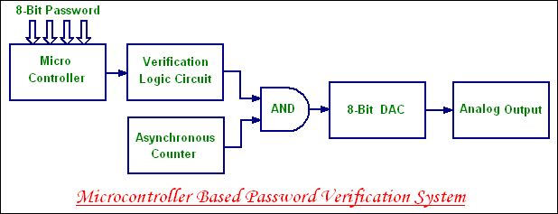
An 8-bit password is the input to this system (A simple example has purposely been dealt with here for the convenience of an average student. The student may modify the circuit and program to try 16 or higher bit password input as an intellectual exercise). In the first section of the circuit the password entered by the user (user-password) is compared with the actual password (password set in the microcontroller using the microprogram) by the microcontroller. The result of the comparison process is an 8-bit output at the output port, which is fed to a logic circuit. If the user-password is correct, the output of the logic circuit will be high. The high output of the logic circuit enables the AND gate in the next section, which has an asynchronous counter as its second input. The digital output of the AND gate is converted to the corresponding analog voltage using a 12-bit DAC.
A microcontroller is a single chip microcomputer, which contains CPU, ROM/ EPROM, RAM and I/O ports. The main features of 8051 microcontroller are: -
- 8-bit CPU optimized for control applications,
- extensive Boolean processing capabilities,
- 64K Program Memory address space,
- 64K Data Memory address space,
- 4K bytes of on-chip Program memory,
- 128 bytes of on-chip Data RAM,
- 32 bi-directional and individually addressable I/O lines,
- two 16 bit timers/ counters- Timer 0 and Timer 1,
- Full Duplex serial port,
- 6-source/ 5-vector interrupt structure with two priority levels and
- On-chip clock oscillator.
Memory can be extended using external EPROM and RAM. 8051 contains an ALU, Timing and Control Unit, Accumulator, B register, PSW (Program Status Word), Stack Pointer, Data Pointer, Timer Registers, Serial Buffer, Program Counter, RAM Address Register, Program Address Register, Instruction Register, Control Registers etc. 8051 is a 40-pin chip operating with 12MHz clock and a single +5V supply. The 8051 has 111 instructions: 49 single byte, 45 two-byte and 17 three-byte.
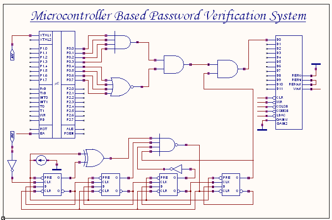
The comparison operation within the microcontroller is performed by means of instructions fed to it known as microprogram. The microprogram constitutes instructions called microinstructions. Our microprogram has microinstructions for setting the password as 0x21 and comparing it with the user-password. If the user-password is correct, the port- P0 gives 8-bit digital output equivalent to 0x0F. If not, the output will be 0xFF and the user again has the option to enter the password. The output of the microcontroller (8-bit digital output) is fed to a logic circuit, which consists of a four input AND gate and a four input NOR gate and an AND gate. The lower order four bits of port- P0 of the microcontroller are fed to the AND gate so that its output is high only when all the four lower order bits are high. The higher order four bits of port- P0 are connected to the NOR gate so that its output is high only when all the four higher order bits of P0 are low. These two outputs are fed to the AND gate which produces a high output only when both its inputs are high. In other words, the output of the logic circuit is high only when the user-password is correct.
The high output of the logic circuit enables the AND gate in the next section. The asynchronous counter is realized using D-Flip-flops, inverters, four-input NAND gates and XOR gate as shown in the circuit diagram. The asynchronous counter output is passed to the Digital to Analog Converter (DAC) through the AND gate only when the password entered is correct. As the counter counts, an equivalent analog voltage is generated using the DAC.
The Digital to Analog Converter used here is LTC1450CG. This device has 12 input data pins. This DAC has an output buffer amplifier, reference (voltage) and a
double buffered parallel digital interface. The digital data is fed to twelve data lines. The analog output voltage is obtained from the Vout pin. Depending upon the logic state of the CLR, WR, CSLSB, CSMSB and the LDAC pins, the input data is loaded and latched into the 12 bit DAC latch present within the DAC. The output buffer is configured such that the gain is 2 by setting the Gain/Gain2 pin to ground. The analog voltage from the DAC (i.e. the output of the whole system) indicates the correct entry of password. Otherwise, the DAC output is null. Thus the microcontroller performs the password verification.
Microprogram:
The microinstructions for the microcontroller are written using the instruction set of 8051. Opcodes for these microinstructions are obtained from the 8051 datasheet. These opcodes are converted to the binary format having the .bin file extension. The .bin file for the microprogram can be created by running the code (in any C compiler) given in GenerateBinary.txt in the \Tools folder of the supplied CDROM. The .bin file is fed as input to the microcontroller so that it can execute these instructions.
Procedure: -
EDWinXP -> Schematic Editor: The circuit is captured in the Schematic Editor in the form of a Schematic Diagram by loading components from the library. Wiring and proper net assignment is made as per the circuit diagram. Values are assigned.
for relevant components.
EDWinXP -> Mixed Mode Simulator: The circuit is preprocessed. The input to the microcontroller is fed as a binary file. To load the binary file proceed in the following manner. From the Component Parameter window for the microcontroller click Setup->Load Binary File->Browse for the psswd.bin file in the Job directory (in this case it is
provided in the job directory; it can be loaded in any of the directories say for e.g.: Lib or Eds_mod. The user may click on the Disassembler button in the above mentioned Set up window to verify the microprogram). ->Exit->Accept. The user can enter the password for verification using the Preset Logic State-> High or Low markers at the port-P1. The clock information for the crystal is set using Preset Logic State-> Clock Generator and the EA input for 8051 is set high using the Preset Logic State marker. Proper parameter assignment is made for the logic gates. In the case of 12-bit DAC, the output of the logic circuit is fed as input to one of the DAC data pins and the remaining 11 input data pins are kept at logic low. In order to set the gain of the amplifier within the DAC as 2, the Gain1/Gain2 pin of the DAC is grounded. Appropriate Preset Logic State markers for the active low pins such as CLR, WR, CSLSB, CSMSB and LDAC are assigned. The waveform markers are placed at the outputs of the microcontroller, the logic circuit, the counter and the DAC. GND net is set as the reference net. The Transient Analysis parameters are also set and the Transient Analysis is executed. The output waveforms are observed in the Waveform Viewer.
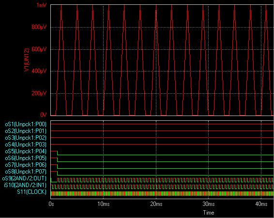
Result: -
The output waveforms observed in the waveform viewer are shown.