Loading the Components
Before we start loading components on the page, turn ON **Grid
(Grid is the dot raster which when enabled, helps in assessing position and
distance while placing graphical item(s)) by enabling the grid from the dropdown,
![]() in
Standard Toolbar. The value for grid may be selected from the drop down list
as .1000”. Similarly, set Snap value to .0500” for better placement
of the components.
in
Standard Toolbar. The value for grid may be selected from the drop down list
as .1000”. Similarly, set Snap value to .0500” for better placement
of the components.
| **Grid is the dot raster which when enabled, helps in assessing position and distance while placing graphical item(s) |
Select ![]() Components from Tools toolbar and right click on the workspace to popup a set
of Component editing tools. By default,
Components from Tools toolbar and right click on the workspace to popup a set
of Component editing tools. By default, ![]() Relocate tool is enabled.
Relocate tool is enabled.
Creating circuit diagram of HALF ADDER:
1. Right click in the workspace and select ![]() Add Components to the Circuit, now click on the option too
Add Components to the Circuit, now click on the option too ![]() Add Components by name from the popup menu. This opens up an input box, enter
7408, (the **Part name of AND gate) and click the ACCEPT button to return to
the workspace with the component attached to your cursor. Click on the workspace
to place it. A copy of the component is still attached to the cursor, so that
the component may be repeated. Since only one instance is required, press ESC.
A-label is attached to the components placed indicating the component name.
In the same way load 7486. Steps 2) 3) and 4) describe another method of loading
components.
Add Components by name from the popup menu. This opens up an input box, enter
7408, (the **Part name of AND gate) and click the ACCEPT button to return to
the workspace with the component attached to your cursor. Click on the workspace
to place it. A copy of the component is still attached to the cursor, so that
the component may be repeated. Since only one instance is required, press ESC.
A-label is attached to the components placed indicating the component name.
In the same way load 7486. Steps 2) 3) and 4) describe another method of loading
components.
![]() Selecting
Selecting
![]() Add
Components by name tool and specifying the X, Y position together with the angle
of rotation will place a single component at the exact location.
Add
Components by name tool and specifying the X, Y position together with the angle
of rotation will place a single component at the exact location.
You may also load components from Library Browser which provides options for multiple loading of components, searching for a component, viewing the details of components, etc.
**Part Name is the name by
which a component is available in the market , it is also called ordering
information In EDWinXP components are loaded with their Part
names rather than the symbol names like INV, 2NAND etc |
2. To load 7408 from Library Browser, right click and select
![]() Add
Components to the Circuit and then click on the option tool
Add
Components to the Circuit and then click on the option tool ![]() Browser to add components tool. Select Parts tab from Library
Browser window that appears. Type 7408 in the Name field. Select 74TTL.PART
from the drop down of Library field and click FIND NOW. The
search results will be listed below.
Browser to add components tool. Select Parts tab from Library
Browser window that appears. Type 7408 in the Name field. Select 74TTL.PART
from the drop down of Library field and click FIND NOW. The
search results will be listed below.
Drag the item in the list and Drop it on to the Schematic (or right click on the selected items and press Send to / Schematic). Setting all options provided in Library Browser narrows search. For more details on Library Browser, please refer EDWinXP Help. In the same way search for7486. Now the list contains 7408 and 7486. Multi- select both by pressing the SHIFT/CTRL key. Right click, to popup a menu.
Select Send to / Schematic. You will find the Parts placed at X, Y (0, 0) location (by default it is at page datum) in the Schematic. The selected components may also be dragged and dropped to the workspace. If one is not familiar with Part names, select Symbol tab, enter the symbol name, i.e. 2AND, and press Find Now. A list of symbols with the name 2AND appears. Right click on one symbol and select Used by Part / ALL LIBRARIES. A list of parts using the symbol appears; load any on the Schematic using the methods described above.
3. Another method of loading components is by using the Library
Explorer, which can be launched by, right click in the Schematic Editor ->
![]() Add
Components to the Circuit, select the submenu
Add
Components to the Circuit, select the submenu ![]() Explorer to add components. This is similar to Windows Explorer
and it shows all the libraries available in the default Library path. Select
the library, 74TTL.PART and select the parts 7408 and 7486 (press Ctrl key and
select with left mouse click) and load into the workspace by Drag drop / Send
to menu in the right click popup menu.
Explorer to add components. This is similar to Windows Explorer
and it shows all the libraries available in the default Library path. Select
the library, 74TTL.PART and select the parts 7408 and 7486 (press Ctrl key and
select with left mouse click) and load into the workspace by Drag drop / Send
to menu in the right click popup menu.
4. Another method of loading components is by using
the component browser, which can be launched from View->Schematic->Browser
(Refer Fig. 4.6). The required components can be obtained either by using
the Browse option in the window or by Search for the element in the quick
menu. Once the element is found, it can be placed in the workspace using
the Place button in the bin. Hotkeys can also be assigned to element names
by which quick launch of components is possible.
|
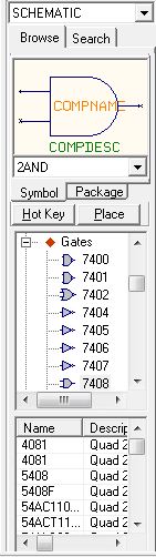 Fig. 4.6 |
5. Half adder needs to make connections to a voltage source, Ground and signal generators for the two inputs. These are external sources (which will not be housed on the PCB) and hence connections to them can be shown with the help of connectors. Take Library Browser to get the pop up window as shown in Fig. 4.7 and type '* 'in the Name field and '*connector*' in the Description field as shown below and press Find Now. The Library Browser will display all the components in the Library with the word connector in its Description (which is entered at the time of Part creation). In the list of parts that appear, select LIST6 since we 6 input output connections.
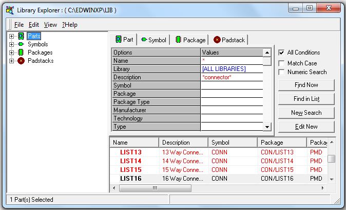
Fig. 4.7
Load the connector and using  Repeat Component function tool, create 5 more instances. Similarly load
SPL0 (Hotkey G) and SPL1 by typing these names in Function tool
Repeat Component function tool, create 5 more instances. Similarly load
SPL0 (Hotkey G) and SPL1 by typing these names in Function tool ![]() Add Components to the Circuit and its option tool
Add Components to the Circuit and its option tool ![]() Add Components to the Circuit and its option tool Add components by
name (F3).
Add Components to the Circuit and its option tool Add components by
name (F3).
6. To relocate the component, right click and select tool ![]() Relocate. Position the part where required and click the mouse to place component.
When you relocate a component from a cluster of components, all other components
present may disappear. Clicking
Relocate. Position the part where required and click the mouse to place component.
When you relocate a component from a cluster of components, all other components
present may disappear. Clicking ![]() Redraw tool brings the components in view again. The component entries must
be placed on the grid for effective wiring. Proper selection of Grid and Snap
value is a must.
Redraw tool brings the components in view again. The component entries must
be placed on the grid for effective wiring. Proper selection of Grid and Snap
value is a must.
![]() Tip
Tip
a) Components may be relocated using bullets. To select (bullet)
a component, press Ctrl key and click on the component. Bullet gets placed on
the component and its function is Relocation. Move the mouse over the bullet.
Now the mouse pointer will change to ![]() move pointer. Click on the bullet and drag to required position.
move pointer. Click on the bullet and drag to required position.
b) You may use Shift + Z to get a full screen cursor that aligns the symbol on workspace while any operation such as relocation, repeat is performed.
c) Pressing the SHIFT key while relocating/ stretching an item, overrides snap value set allowing the item to move/ stretch smoothly.
***Instead of using Right click
menu for selecting function tools, they may also be activated from their
toolbars which are by default placed on the left of the workspace. These
toolbars are dock able, i.e. they may be relocated and placed anywhere
on the editor window. To lock toolbar position select Preferences / Lock
toolbar (CTRL + H). |
7. With the Function tool ![]() Relocate selected, click on 7408 to select it. The AND gate gets highlighted,
now move the cursor and press left mouse button (or SHIFT + ENTER) to fix the
component at that location. Repeat the same procedure with 7486.
Relocate selected, click on 7408 to select it. The AND gate gets highlighted,
now move the cursor and press left mouse button (or SHIFT + ENTER) to fix the
component at that location. Repeat the same procedure with 7486.
The Parts are placed as shown in Fig. 4.8. The connectors have been placed in
such a way that the end pins, 1 and 6 are devoted for Power/Ground signals.
On packing the pin number to which the entry corresponds to will appear (refer
the picture, all the numbers in grey are the corresponding pin numbers in the
package).
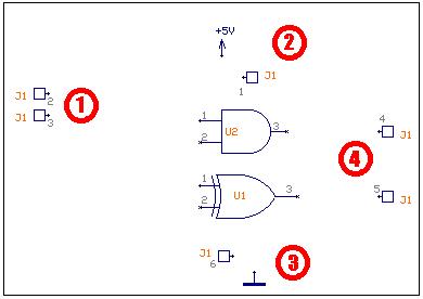
Fig. 4.8
Half adder has six different signals, i.e., A,B,SUM,CARRY,Vcc
and GND. In EDWin XP common terminology for Vcc (+5V) is SPL1 and GND is SPL0.
The printed circuit board requires connections to signal generators for A and
B, these can be made by connectors shown near .location marked 1 in the picture
above,
location marked 2 is for making connections to SPL1, 3 for SPL0 and 4 for output
connections (for signals SUM and CARRY).
![]() Please refer
EDWinXP / Help / Show me How / Schematic Editor / Component editing tools to
view movies illustrating the methods described.
Please refer
EDWinXP / Help / Show me How / Schematic Editor / Component editing tools to
view movies illustrating the methods described.