Full Adder
Aim
To simulate a 3-bit full adder circuit.
Components
Name |
EDWin Components Used |
Description |
Number of components required |
| AND | 7408 | 2-input AND gate | 3 |
| OR | 7432 | 2-input OR gate | 2 |
| XOR | 7486 | 2-input XOR gate | 2 |
| CLOCK | SMB_CLOCK | Clock | 1* |
Theory
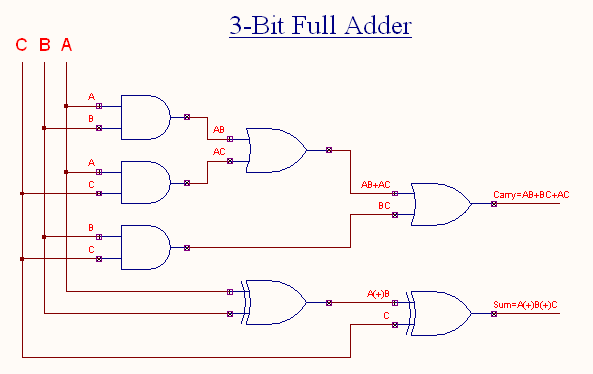
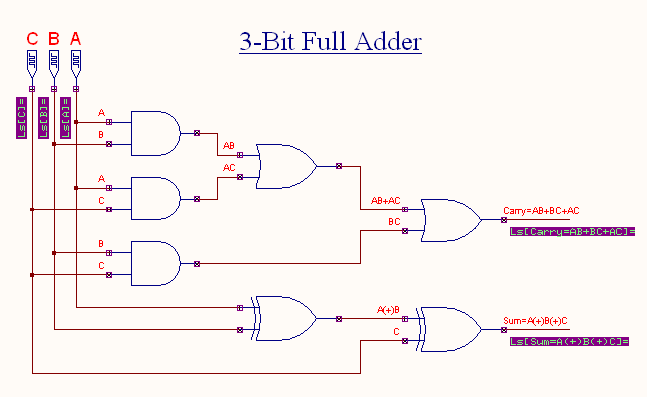
The circuit diagram of a 3-bit full adder is shown in the figure. The output of XOR gate is called SUM, while the output of the AND gate is the CARRY. The AND gate produces a high output only when both inputs are high. The XOR gate produces a high output if either input, but not both, is high. The truth table of 3-bit full adder is given. The 3-bit full adder circuit has a provision to add the carry generated from the lower order bits.
Input |
Output |
|||
C |
B |
A |
Sum |
Carry |
0 |
0 |
0 |
0 |
0 |
0 |
0 |
1 |
1 |
0 |
0 |
1 |
0 |
1 |
0 |
0 |
1 |
1 |
0 |
1 |
1 |
0 |
0 |
1 |
0 |
1 |
0 |
1 |
0 |
1 |
1 |
1 |
0 |
0 |
1 |
1 |
1 |
1 |
1 |
1 |
Truth Table
![]()
![]()
Proof
![]()
![]()
![]()
![]()
![]()
![]()
![]()
Procedure
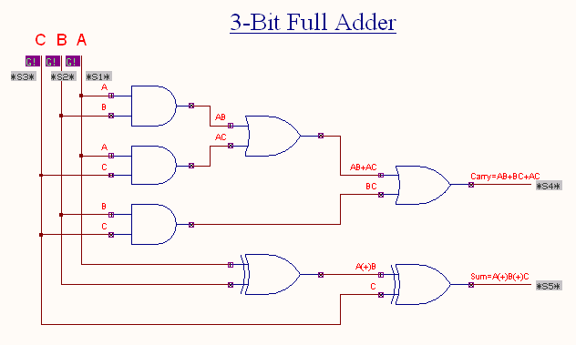
EDWinXP -> Schematic Editor: The circuit diagram is drawn by loading components from the library. Wiring and proper net assignment has been made.
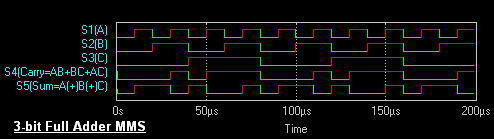
EDWinXP-> Mixed Mode Simulator: The circuit is preprocessed. The clock input for all A, B and C is set. The logic waveform markers are placed at the A, B and C inputs, and the Sum, Carry outputs of the circuit. The Transient Analysis parameters are also set and the Transient Analysis is executed. The output waveform is observed in the Waveform Viewer.
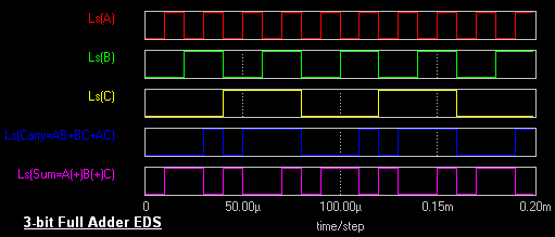
EDWin 2000 -> EDSpice Simulator: The circuit is preprocessed. The clock input for all A, B and C is set by attaching the corresponding Digital
Input Vector file. The logic waveform markers are placed at the A, B and C inputs, and the Sum, Carry outputs of the circuit. The Transient Analysis
parameters are also set and the Transient Analysis is executed. The output waveform is observed in the Waveform Viewer.
Result
The output waveform is observed in the waveform viewer.