PCB Layout Editor
Arc insertion in polygon: Click Here
Highlighting of component and nets
Feature:
- Instant highlighting component and nets in Layout and Schematic
This feature is prominent while displaying visualization on dual monitor.This feature can be availed only if both the Schematic and Layout editors are opened up.This feature is more effective in dual monitors. Load an EDWinXP project and open Schematic and Layout.
For component highlighting:
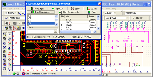
From Layout editor, select option General from Info menu bar items; a dialog box with general information regarding the objects placed on the workspace will pop up. Select Layout component tab and click on object to be highlighted from this dialog. The particular item would be highlighted on the Layout workspace as well as in the schematic editor.
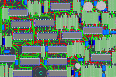
The figure below shows component highlighted both in Layout and Schematic editor at same time. The selected pin will be highlighted with an arrow in both editors. This highlight feature can also be availed from Schematic editor in the similar way.
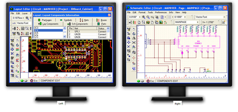
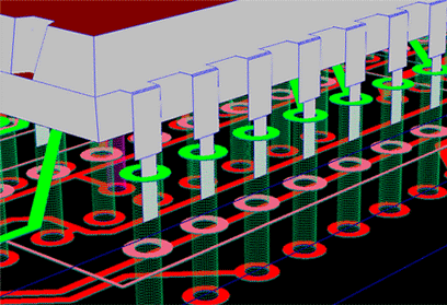
Instant highlighting of components from Layout Editor.
For net highlighting:
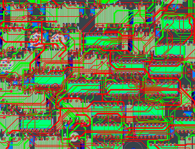
From Layout editor select connection and enable connection property. Click on a net to view its properties. The selected net is highlighted in the Layout editor. The net corresponding to the Layout will be highlighted in the schematic editor simultaneously. The figure below shows nets highlighted both in Schematic and Layout editor at same time.
Instant highlighting of nets from Layout Editor
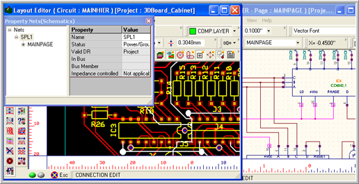
In the Property Nets (Layout) right click a single item. Select redraw of particular pin; the selected pin will be highlighted with an arrow in both the editors.
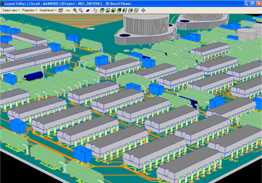
Enhanced 3D Viewer using OpenGL
When this tool is invoked, a separate Layout viewer will be opened which contains the 3D board view of the project. The board can be rotated with the mouse buttons.
- Moving mouse up and down with depressed left mouse button rotates view around X axis.
- Moving mouse left and right with depressed left mouse button rotates view around Y axis.
- Moving mouse left and right with depressed right mouse button rotates view around Z axis.
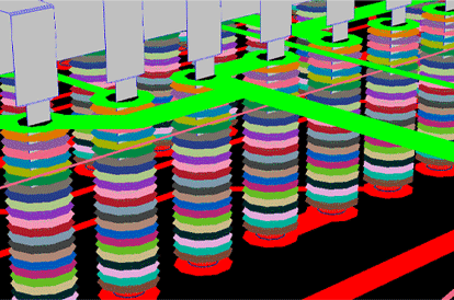
3D Board View
3D Board Top View
3D Board Bottom View
Improved 3D Visualisaton
Previous version of three-dimensional visualization has been replaced entirely with OpenGL. Advantages are faster response time with scrolling, rotating and zooming of the scene. Quality of rendered view has been significantly improved. Rendered scene has been (with exception of Library Editor) moved to separate window. It is now possible to view and edit boards in 2D and 3D simultaneously. New 3D visualization covers the way the 3D cursor and objects are relocated in the space and navigated through the scene. There are three detail levels of visualization (low, medium and high) where low is more or less the same as visualization quality in previous version. Preparation for high detail level visualization may take some time depending on complexity of the board and computer speed.
Usage of mouse buttons and Navigation through 3D scenes
Left button
- To rotate the scene around X-axis hold left mouse button depressed and move cursor vertically up or down.
- To rotate the scene around Y-axis hold left mouse button depressed and move cursor horizontally to left or right.
Right button
- To rotate the scene around Z-axis hold right mouse button depressed and move cursor horizontally to left or right.
Middle button / mouse wheel
- To pan (scroll) the scene hold middle button depressed and move cursor in any direction.
- Turn mouse wheel backwards to zoom in, forward to zoom out.
Relocation
Left button
Using SHIFT or ALT key +LEFT CLICK moves crosshair cursor horizontally to left or right and vertically to up or down in the X-axis .
Movement to the right increases X-coordinate of the cursor and movement to the left decreases.
Using SHIFT or ALT key +LEFT CLICK moves crosshair cursor vertically up or down in the Y-axis. Upward movement increases Y-coordinate of the cursor and downward movement decreases.
In addition, the displacement of the cursor and items are also dependent on snap and grid values set.
With SHIFT key depressed 3D cursor moves by steps defined in “Snap” dropdown box.
With ALT key depressed cursor moves by steps defined in “Grid” dropdown box.
Right button
Using SHIFT or ALT key + RIGHT CLICK moves crosshair cursor vertically up or down in the Z-axis. Upward movement increases Z-coordinate of cursor and downward movement decreases.
With SHIFT key depressed 3D cursor moves by steps defined in “Snap” dropdown box.
With ALT key depressed cursor moves by steps defined in “Grid” dropdown box.
Object selection
Single object selection
Point to one of the vertex (corner) with crosshair cursor and double click left mouse button for single object selection. Selected object is highlighted and can be interacted with currently active function tool. A double click on the screen or click on icon in Options Toolbar finishes the editing operation.
Multiple objects selection ( for relocation ,deletion)
Double clicking all + CTRL key selects a group of objects. The last object in the group must be double clicked without
Ctrl key upon which currently active editing operation may commence. Each selected object is highlighted.
A double click + CTRL key disables objects that have been added to the group.
3D Trace View
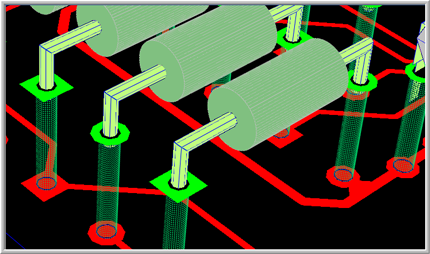
3D Trace View with All Active Layers Enabled
3D Trace View With Active Layers in Set to used Condition
Introduction
PCB wizard is a new tool which helps EDWinXP users to create the board in few steps. It facilitates automatic placing and routing of components . Proper settings have to be done on each step for the perfect completion of the board.
Procedure:
The components of the schematic are packed either by manual or auto packaging. Then invoke the Layout Editor. The packaged components will be stacked at the board datum.
Select Tools -> PCB Wizard. A window will be popped up as shown below.
The required board parameters are to be entered in the fields.
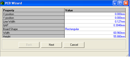
Click Next.
The parameters for autoplacing are set according to the requirement in the next window. The circuit design rules can be set in the section for Design rules.
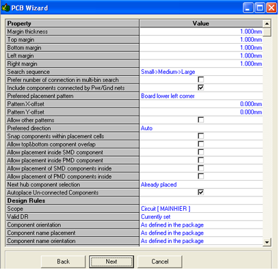
Click Next.
Note: There should not be any component left outside the board before routing. All the copper items and copper pour areas should be placed inside the board manually. In the next window, if no separate routing parameters are provided, the PCB wizard will take the default values from the circuit design rules to place and route the board.
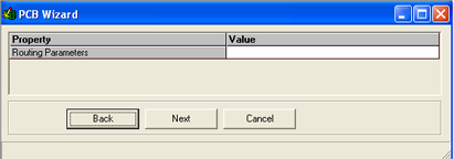
You can also browse and input the routing parameters if necessary. The parameters can also be changed/ edited from the Routing Parameter Settings window.
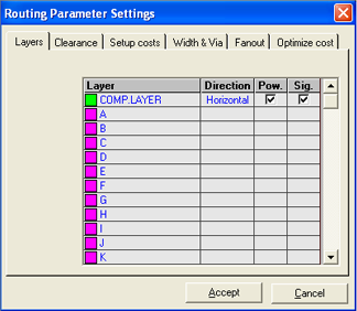
If any routing parameter is changed and when the Accept button is clicked, it will prompt to override rules specified in Circuit Design Rules.
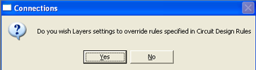
Click on Yes
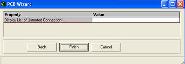
After the completion of the automatic placing and routing, if any unrouted connections are present, it will list in the Display List of Unrouted Connections field. Click on Finish to exit the PCB wizard.