Added cross lines in Long Cursor.
1. Select EDWinXP → PCB Layout Edit → PCB Layout → View → Long cursor
2. Select the Long cursor option from the menu it will enable
3. After click on this option, go to Tools → Connections a new dotted line cursor will be there to draw the Traces in 45 degree more easily
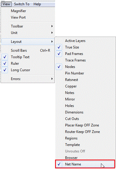
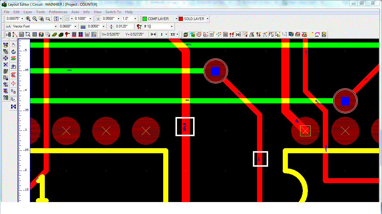
Display of NetNames on Trace (On/Off)
In Layout Editor display the Net Names of each nets for identification.
1. Select EDWinXP → PCB Layout → PCB Layout → View → Layout → Net Name
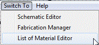
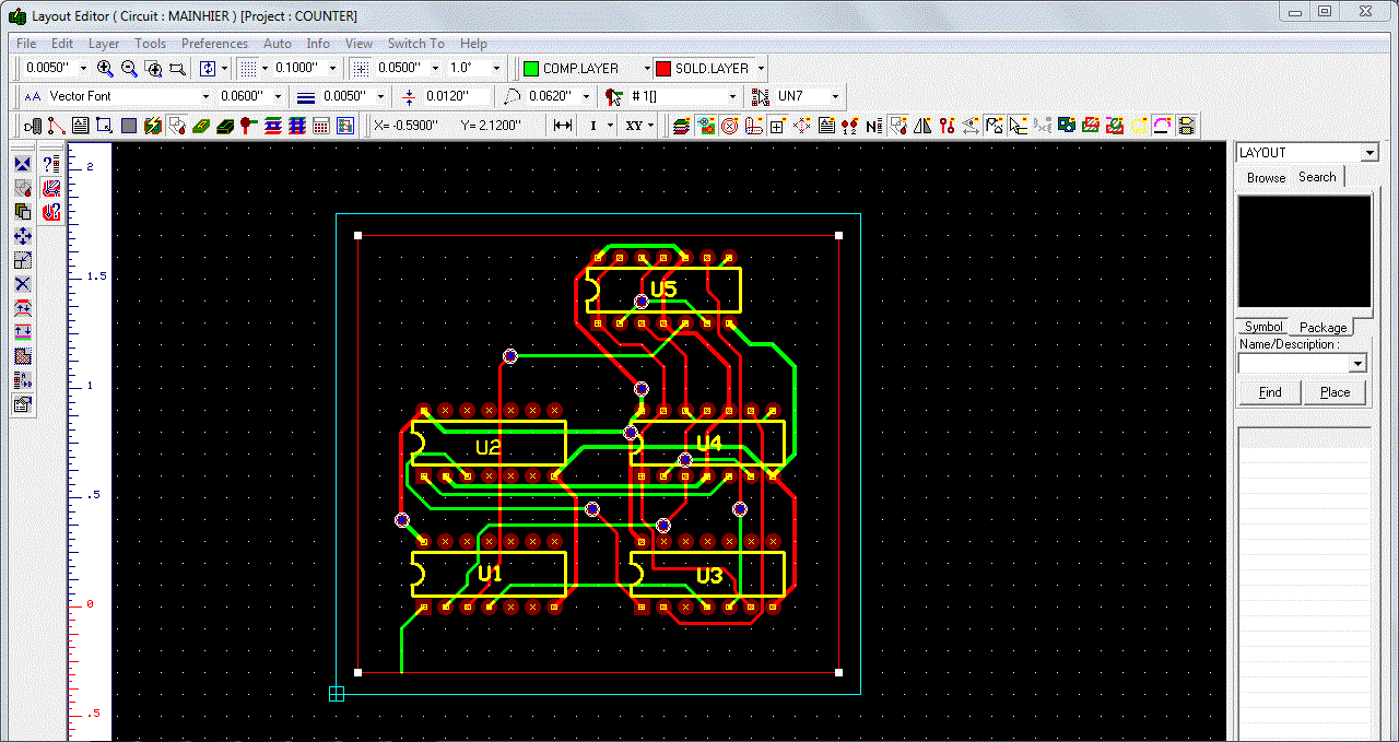
Switching between Layout Editor , Fabrication Manager and List of Materials Editor.
1. In order to switch to Layout Editor , Fabrication Manager and List of Materials Editor , select Switch To menu → Layout Editor or Fabrication Manager or to List of Materials Editor
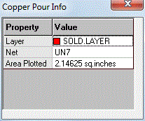
Calculate the total area plotted by the copper pour area.
1. Select EDWinXP-Main → PCB Layout → Tools menu → Copper.
4. Select Copper Item property  → Display Copper pour info
  . A popup window will appear containing the copper Pour Info.
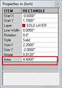
Calculate area of Copper Plane
1. Select EDWinXP-Main → PCB Layout → Tools menu → Copper.
2. Select Create graphic Item  → Create Rectangle
 .
.
3. Press Ctrl + Right click on mouse → Select Properties → Copper. A pop up window will appear which contains the total area of the copper plane.