Bridge Rectifier
Aim
To simulate a Bridge Rectifier circuit.
Components
Name |
EDWin Components Used |
Description |
Number of components required |
| TRANSFORMER | TRANSFORMER | Transformer | 1 |
| RES | RC05 | Resistor | 1 |
| DIODE | 1N4007 | Diode | 4 |
| VGEN | VGEN | Ac voltage source | 1 |
| GND | SPL0 | Ground | 1 |
Theory
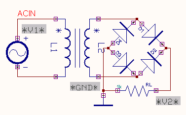
The Bridge rectifier is a circuit, which converts an ac voltage to dc voltage using both half cycles of the input ac voltage. The Bridge rectifier circuit is shown in the figure. The circuit has four diodes connected to form a bridge. The ac input voltage is applied to the diagonally opposite ends of the bridge. The load resistance is connected between the other two ends of the bridge. For the positive half cycle of the input ac voltage, diodes D1 and D3 conduct, whereas diodes D2 and D4 remain in the OFF state. The conducting diodes will be in series with the load resistance RL and hence the load current flows through RL. For the negative half cycle of the input ac voltage, diodes D2 and D4 conduct whereas, D1 and D3 remain OFF. The conducting diodes D2 a nd D4 will be in series with the load resistance RL and hence the current flows through RL in the same direction as in the previous half cycle. Thus a bi-directional wave is converted into a unidirectional wave.

Peak Inverse Voltage
Peak inverse voltage represents the maximum voltage that the non- conducting diode must withstand. At the instance the secondary voltage reaches its positive peak value, Vm the diodes D1 and D3 are conducting, where as D2 and D4 are reverse biased and are non-conducting. The conducting diodes D1 and D3 have almost zero resistance. Thus the entire voltage Vm appears across the load resistor RL. The reverse voltage across the non-conducting diodes D2 (D4) is also Vm. Thus for a Bridge rectifier the peak inverse voltage is given by
![]()
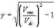
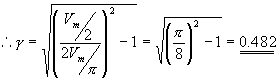
Ripple Factor
The ripple factor for a Full Wave Rectifier is given by
The average voltage or the dc voltage available across the load resistance is
![]()
![]()
![]()
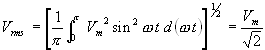
RMS value of the voltage at the load resistance is
Efficiency
Efficiency, h is the ratio of the dc output power to ac input power
![]()
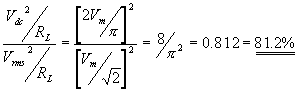
The maximum efficiency of a Full Wave Rectifier is 81.2%.
Procedure
EDWinXP> Schematic Editor: The circuit diagram is drawn by loading components from the library. Wiring and proper net assignment has been made. The values are assigned for relevant components.
EDWinXP -> Mixed Mode Simulator: The circuit is preprocessed. The test points and waveform markers are placed in input and output of the circuit. GND net is set as reference net. The Transient Analysis parameters have been set. The Transient Analysis is executed and output waveform is observed in Waveform Viewer.
Result
The output waveform may be observed in the waveform viewer.
