BJT input characteristics
Aim: -
To design and simulate a BJT input characteristics.
Components: -
Name |
EDWin Components Used |
Description |
Number of components required |
| VDC | VDC | DC Voltage Source | 3 |
| GND | SPL0 | Ground | 1 |
| NPN | BC107 | Transistor | 1 |
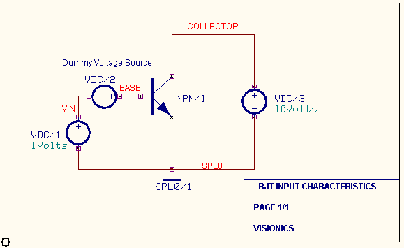
Circuit Diagram: -
Procedure for creating schematic diagram and simulating it
- 1. Open EDWinXP x.xx from Start -> Programs -> EDWinXP Main
- 2. Invoke the Schematic editor by double clicking the Project ->; Main page
- 3. Choose EDSpice Simulator from Preferences Menu
Loading/Placing of components
- 1. In Browser, Select Transistors and choose Transistor, click on place button and place it on the screen.
- 2. Select Ground from Sources group and place it.
- 3. Select DC Power supply (VDC) from Sources group and place it.
- 4. The components can be placed in the grids with 100 mils (.1") and snap of 50 mils (.05")in the required position by relocation.
- It is possible to use the customized keyboard keys for easy placement of components.
- Eg: G for ground, E for DC Power supply, Q for transistor e.t.c
- F1 to rotate
component F4 to End connection
Routing Connections
- 1. The connection between components can be made by Preferences -> Instant net name, Instant wire label ( make enable)
- 2. Tools-> Connections->Connect components (First Function tool) {Connect the wires from pin to pin according to the circuit diagram.} while asked for entering Net name, give suitable names
- 3. Select Tools->Connections->Connection properties (Seventh function tool) ->Click on any connection and name it as required.
- Do not rename SPL0 (Ground)
Giving values
- 1. Tools ->Components -> Component properties -> Change simulation parameters->Select any component and change it values.
- 2. Click on the DC Power Supply.
- A window is pops up
- 3. Enter following values
- DC and Transient analyses value of the source [DC/TRAN] - 1 volts
- 4. Click Accept
Similarly Set VDC/2 as 0 volts and VDC/3 as 10 volts
Simulation
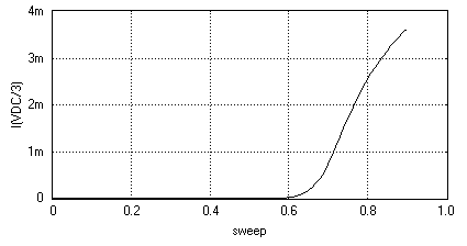
Note: For input/output characteristics plot of BJT, FET, MOS etc, it is not necessary to place a waveform marker in the diagram. Its because the sweep variable of the VI parameters are being plotted. The current through a net can be obtained by enabling the Vx#branch in the waveform. Please ensure the connectivity of dummy voltage source having (0V) for obtaining the direction of current.
-
1. Simulation -> Preprocess
- 2. For setting up simulation time and analysis types, select Simulation menu, choose Analysis.
- 3. In the window pops up, select DC Transfer function analysis from tree view.
- 4. Enter following values:
- First Source - VDC/1 [V2]
- Start voltage - 0
- Stop voltage - 900m
- Step - 10m
- Results : Select waveform from drop down menu.
-
5. Click on Accept.
- 6. Expand the DC transfer function and select Waveform viewer,
- 7. Select dummy voltage source branch.
- 8. Click on Accept.
-
9. Select DC Transfer function analysis
-
10. Run Analysis by clicking on Run button
- 11. Verify the results
Result:-
The output waveform may be observed in the waveform viewer.